作者姓名:LUCY, LUCY

Cross-section of a multilayer circuit board next to inner-layer cores and prepreg, illustrating the PCB lamination process used to bond multilayer boards
Blog

PCB Lamination Process: How Multilayer Circuit Boards Are Bonded

This guide is for PCB designers, NPI engineers, and hardware teams who specify multilayer boards and need a clear picture of how lamination bonds cores, prepreg, and copper. It separates layer count from real stack-up decisions, and it shows which construction, material, and via choices to lock before the press makes them permanent.
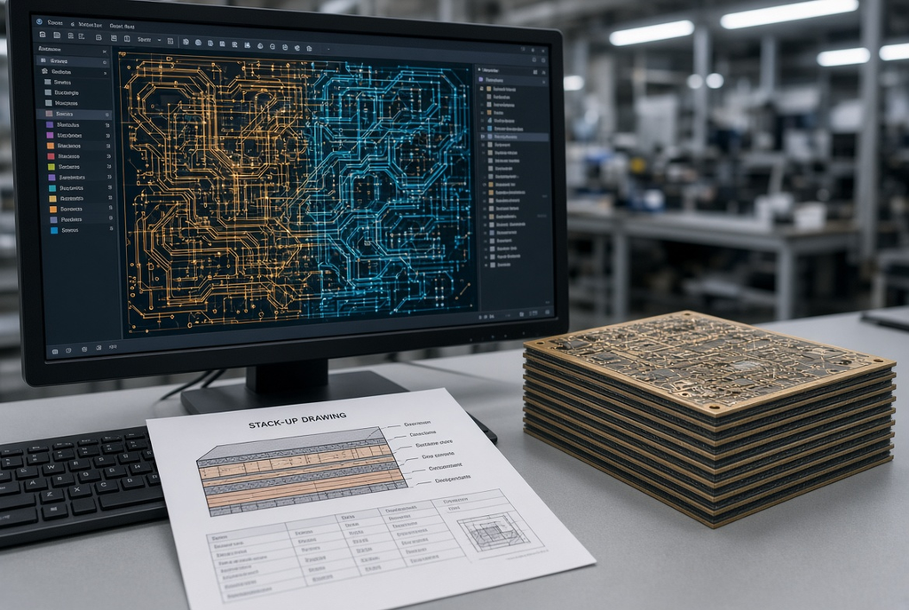
PCB manufacturing process thumbnail showing Gerber fabrication data on a monitor next to finished bare circuit boards, representing the path from design files to a released bare PCB.
Blog

PCB Manufacturing Process: From Gerber Files to Finished Circuit Boards

This guide walks PCB designers, NPI engineers, and sourcing staff through the path from Gerber files to a finished bare board. It explains why a fabrication data package must define revision, stack-up, drill, finish, and test intent, how CAM and DFM review happens before material is cut, and which factory stages and release checks you should agree before production starts.

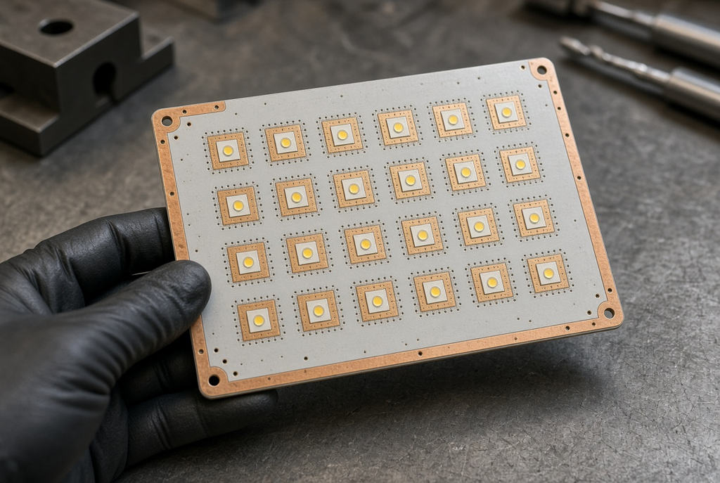
Metal-core LED PCB with thermal vias and LED pads showing the thermal path from package to board for lighting applications
Blog

What Is an LED PCB? Materials, Thermal Design, and Common Applications

Lighting engineers, product developers, and buyers specifying LED boards often treat the PCB as a generic substrate. This article explains how materials and thermal paths decide junction temperature, light output, and life. It covers FR-4, metal-core, and ceramic options, vias and copper spreading, stack-up and layout choices, and common lighting uses so you can brief fabrication and assembly with clearer thermal intent.

Close-up of a printed circuit board showing MLCC, electrolytic, and tantalum capacitors used to identify capacitor types by package and placement
Blog

Circuit Board Capacitors: Types, Functions, and How to Identify Them

Engineers, technicians, and buyers who read boards and BOMs often treat every small part near a chip as the same capacitor. This article clears the mix-up among MLCC, electrolytic, tantalum, and film packages, shows how to identify capacitors on a board by size, polarity, markings, and placement, and flags the substitutions that change decoupling, bulk filtering, and field reliability before assembly.

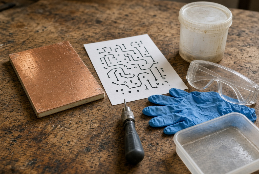
Copper-clad board and toner-transfer print prepared for home PCB etching beside etchant, gloves, and simple tools on a workbench
Blog

How to Print a PCB: Image Transfer, Etching, Drilling, and Finishing

For hobbyists, students, and teachers, “printing” a PCB usually means toner transfer, chemical etching, drilling, and a basic finish. This guide walks through that DIY flow, names the chemicals and risks, and draws a hard line between a classroom board and a product you would ship. Use it before you mix etchant—and stop when the design needs professional fabrication.

Schematic or layout view on a monitor beside a bare printed circuit board and an assembled PCBA, showing the design-to-production workflow
Blog

How to Make a Circuit Board: From Schematic Design to PCB Assembly

Hardware engineers, founders, and buyers often treat board making as routing plus a Gerber upload. This guide maps the full path from schematic to a working assembly—layout and stack-up, fabrication data, component sourcing, and first-article test—so you know which files and decisions to lock before a manufacturer starts the build. It is written for people sending files to a partner, not etching boards at home.

Bare printed circuit board with green solder mask showing pad openings and traces on an inspection table
Blog

Why Are Circuit Boards Green? The Role of Green Solder Mask

This article helps engineers, buyers, and technically curious readers who have always seen green boards and assumed the color was required. It explains what green solder mask actually does in fabrication and assembly, why the industry standardized on green, and how mask color differs from surface finish. You leave knowing which questions to ask before specifying a non-green mask on a real build.

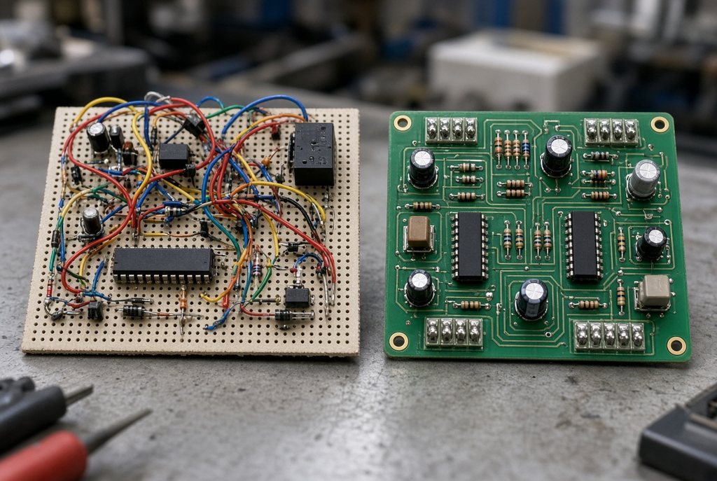
Protoboard with hand-soldered connections beside a custom printed circuit board with defined traces and pads
Blog

Protoboard vs PCB: Key Differences and When to Use Each

Engineers, students, and product developers often keep a working circuit on a protoboard longer than the project can stand. This article separates a generic wiring board from a fabricated custom PCB, shows when each still belongs in a project, and flags the electrical, mechanical, and process risks that appear when a bench prototype is treated as a production board.

滚动至顶部