The PCB lamination process is the part where inner layer, cores and prepreg are fused together under heat and pressure to create a multi-layered construction. Once the press, it’s no longer a CAD note. The thickness, dielectric spacing, copper distribution and via architecture are permanently fixed to the panel. The lack of clarity in construction planning becomes apparent later as warpage, thickness variation, impedance shift, or drill problems – not as a line you can edit in the next Gerber revision.
The number of layers is not the most important factor. A “no material family, copper balance, symmetry or via type” callout of “8-layer, 1.6 mm” still leaves the fabricator with the task of creating a stack. That is a popular source of unnecessary engineering inquiries and reliability concern. This guide details how multi-layer circuit boards are joined up, the types of stack-up decisions that remain after press, and what designers and NPI teams should verify prior to the first lamination cycle.
Multilayer PCBs Start With a Defined Stack-Up, Not Just a Layer Count
A multilayer board isn’t a “4-layer” or “8-layer” board. It is a defined sequence of cores, prepreg and copper that should be clear before stacking up the PCB and laminating. The number of layers is indicative of the number of copper planes available. The stack-up provides the factory with information about the assembly and spacing of those planes and how they are bonded.
Proceed as if the stack-up is a design document. It influences electrical performance, end thickness, drill strategy and mechanical behavior. The factory can make a board if the construction is not included. It could be a different board to what you had in mind.
Core, prepreg, and copper: the building blocks of a multilayer stack
Most work done by 3 materials.
A core is a material that has already been fully cured with copper clad laminate. Inner-layer circuits are printed and etched on cores, which then get lost inside the stack. Prepreg is glass cloth pre-coated with uncured resin. That resin flows, fills and then cures in the press, fusing adjacent copper and dielectric surfaces. The construction of the outer layer copper supply is provided by copper foil.
Typically a 4-layer board consists of one core and two layers of pre-preg and foil. An 8-layer bare board typically includes multiple layers of cores and multiple pre-pregs transitions in order that each copper layer is placed at the desired gap between the other copper layers. These “8-layer” labels can cover a range of very different thicknesses of dielectrics, styles of glass and resins. Those differences alter the impedance, drill action and panel movement of the press.
Why stack-up must be explicit in the fabrication package
The fabrication package is supposed to answer these questions that the press department may not be able to guess: The 8-layer, 1.6 mm FR-4” designation is not sufficient to determine the specific layers or materials used. The fabricator will suggest a construction that will include cores and prepreg that are available. That could introduce a change in the dielectric spacing, a shift in an impedance layer, or an incorrectly positioned copper structure that would become warped during the reflow process.
Electrical, mechanical and manufacturing reviews should be made against the same construction, and should occur early enough in the stack-up to prevent issues. The change in glass style or prepreg count after the release of artwork is not a paperwork edit. It is a new lamination scheme.
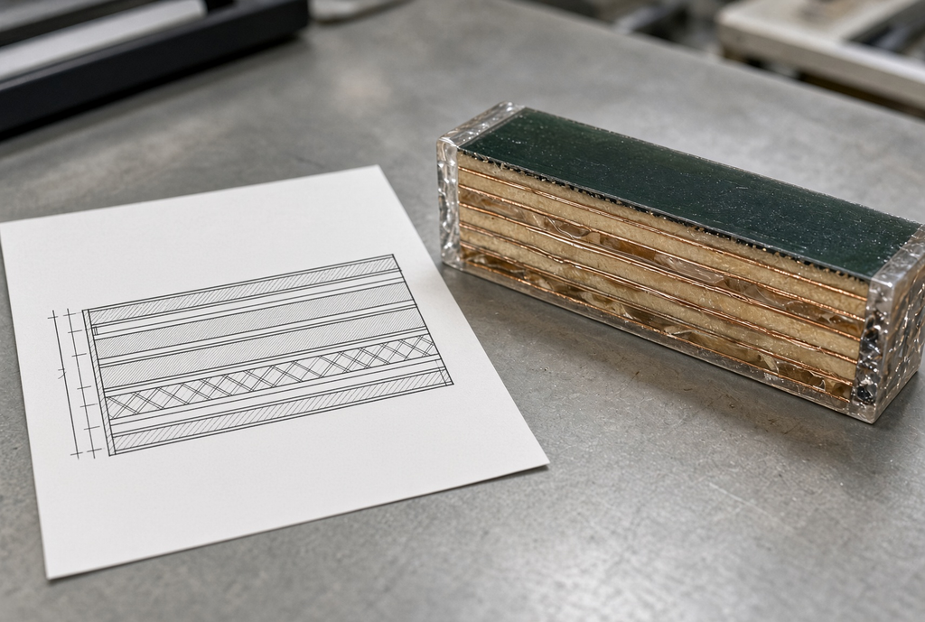
The PCB Lamination Process: From Inner Layers to a Single Board
Shop Order is easier to process than the press recipe. Lower layers are photographed/etched, inspected, and prepreg and outer copper are laid up. The prepreg is squeezed into the stack to flow and cure. The panel then becomes a single board after this. Actually, the inside construction is already stable, and the process of outer layers, drilling, plating and finishing is still in progress.
The designers and buyers don’t need all of the press parameters. They must be aware of what is checked prior to burying the stack, how lay-up errors become voids and/or registration issues, and why the cure step renders the stack-up permanent.
Inner-layer imaging, etch, and inspection before press
The inner copper is subjected to processing and the core remains as a separate sheet. The factory makes the inner graphics, removes unwanted copper and checks it before sealing the layers between the laminate. On a flat inner-layer core, it is easier and less expensive to detect opens, shorts, nicks and incorrect residual copper after the lamination process.
A buried defect is not a defect in the outer layer of the host computer. In many cases, outer copper can be reworked, or in a few cases, repaired. There is an inner-layer error already in the board. A frequent cause of scrap after the press cycle is completed is to assume that it will be resolved after the fact.
Lay-up: arranging cores, prepreg, and outer copper
Lay-up refers to the physical process of building the stack. The inner-layer cores are placed in a first layer, followed by the specified prepreg sheets and outer copper foils are placed in a last layer. The layers are held in register by pins, slots or optical targets. The order is as important as cleanliness. Void, resin debris, or the wrong prepreg style can lead to resin starvation or a local thickness error, which only becomes apparent after cure.
This is the final opportunity to maintain alignment of inner features as per the drill program. After bonding the stack, a very slight movement on a core sheet becomes a broken drill, thin ring, or a missed buried via.
Heat, pressure, and cure: bonding the multilayer construction
The laid-up book is put in a press. Prepreg resin is softened by heat to flow in copper topography and between glass fibres. During that flow the stack is kept closed by pressure. The resin becomes cross-linked to form a solid dielectric at a certain time at temperature. The cycle and profile will be different for various material systems and construction. They are NOT shared numbers; they are not copies of other projects.
In the very literal sense, this is multilayer PCB lamination.In this case, the prepreg is no longer a bonding sheet, but a component of the final dielectric. The board cannot be stacked after cured. There’s no need to add thickness or resin fill or even ensure that the layers are bonded together as those are properties of the panel now, rather than options on a drawing.
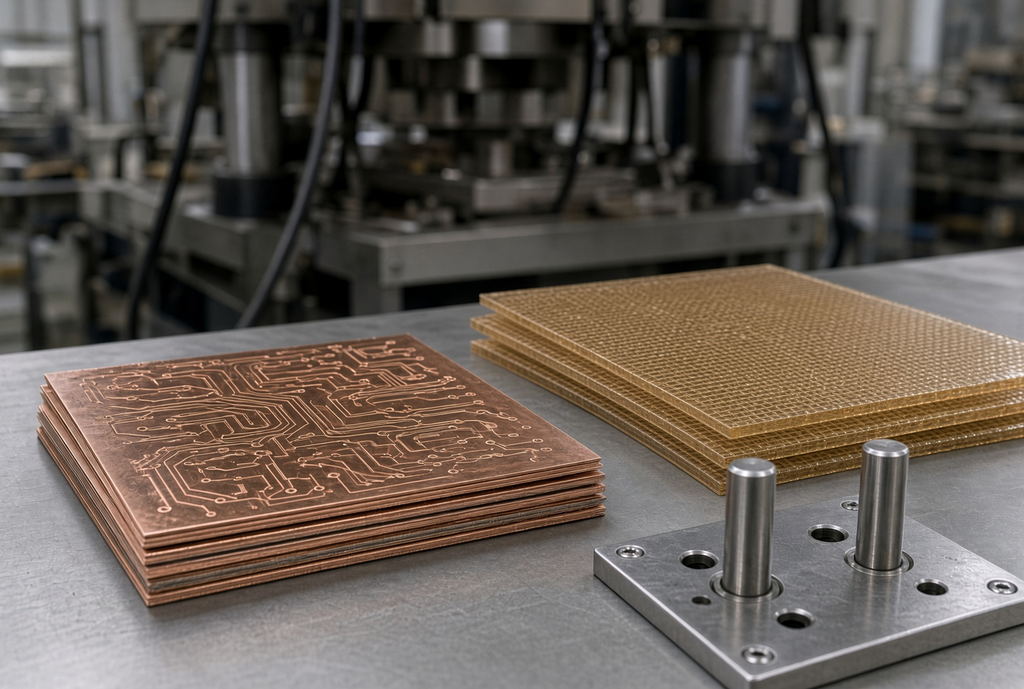
Stack-Up Symmetry and Copper Balance: Hidden Drivers of Warpage and Yield
A stack might be electrically correct, but still laminate poorly. Two of the lesser obvious causes of bowing boards after press and after reflow are asymmetric dielectric build and uneven copper. The electrical netlist doesn’t alert you. The panel does.
What symmetric and balanced stack-ups mean in practice
A symmetric stack up is one that is symmetrical about the center line of the board. The thicknesses of the dielectrics, the glass types and the thickness of the cuprates on one side of the midplane should be the same on the other side. When making up a balance, each corresponding layer must have the same amount of copper, not just one solid layer and the other a sparse pattern.
It’s easy to imagine a 4-layer example. Layer 2 is a thick layer of ground pour. Layer 3 is almost blank other than some traces. The copper-rich side and the copper-poor side of the laminate do not shrink equally after the lamination and reflow process. The panel bows to the audience. That bow becomes a “cosmetic complaint” on a larger board. It’s a problem of assemblies and connectors.
How imbalance shows up after lamination and assembly
Warpage is the obvious symptom. Some less apparent issues are registration problems in SMT, connectors that clash with the outline of the board, mechanical stress at the mounting holes and changing impedances due to the variance in the thickness of the dielectrics on the panel. If heavy copper is placed on one or two layers, the problem becomes sharper because it is the mechanical response of these layers which is dominant.
While the stack-up is in a draft stage, discuss copper balance for multi-layered PCB construction with the fabricator. Extra non-functional copper thieving, extra planes redistribution or prepreg adjustment on both sides of the centerline is cheap on paper.
Material Selection and Thermal Behavior in Multilayer Lamination
Multilayer boards’ material selection is not only a dielectric constant or loss conversation. The flow and cure personality of the resin in the press is the same as the thermal expansion personality in assembly used for the electrical target. Those two behaviours are combined in one review.
Standard FR-4 versus high-Tg, low-loss, and specialty materials
The Standard FR-4 is designed for a variety of commercial multilayer applications. High-Tg materials are used when the board will be used at higher operating temperature and/or more demanding reflow. When high speed or high frequency dictates the choice of the material, low loss materials are specified. Everyone’s family is unique, and everyone’s family has its own flow and healing curve. Resin content, glass style, and filler affect the ability of the prepreg to fill copper features and the movement of the stack during the heat up.
One of the more common mistakes is to list a material family name on the BOM with an ambiguous grade. Two laminates can have the same family label and yet have different flow, glass transition temperature and price. If it is dependent on a specific grade, write the grade down in the space provided: impedance, thickness, or sequential lamination.
Thermal expansion, reflow, and reliability after lamination
Once the board is bonded it still must pass soldering and field temperature cycling. The coefficient of thermal expansion is a material property, and can also vary by direction—specifically from the thickness direction versus in the plane of the glass. When there is a mismatch in expansion between the layers (or between board and large component), the stress is concentrated at the vias and at the bond interfaces formed during the lamination process.
Never use any single Tg or CTE number as a rule of thumb. Such values are for a particular material and construction, and should be matched to the application: the number of reflow passes; the operating temperature; the aspect ratio of the vias; the design type (blind, buried or stacked). The lamination bond only lasts as long as the surrounding thermal plan.
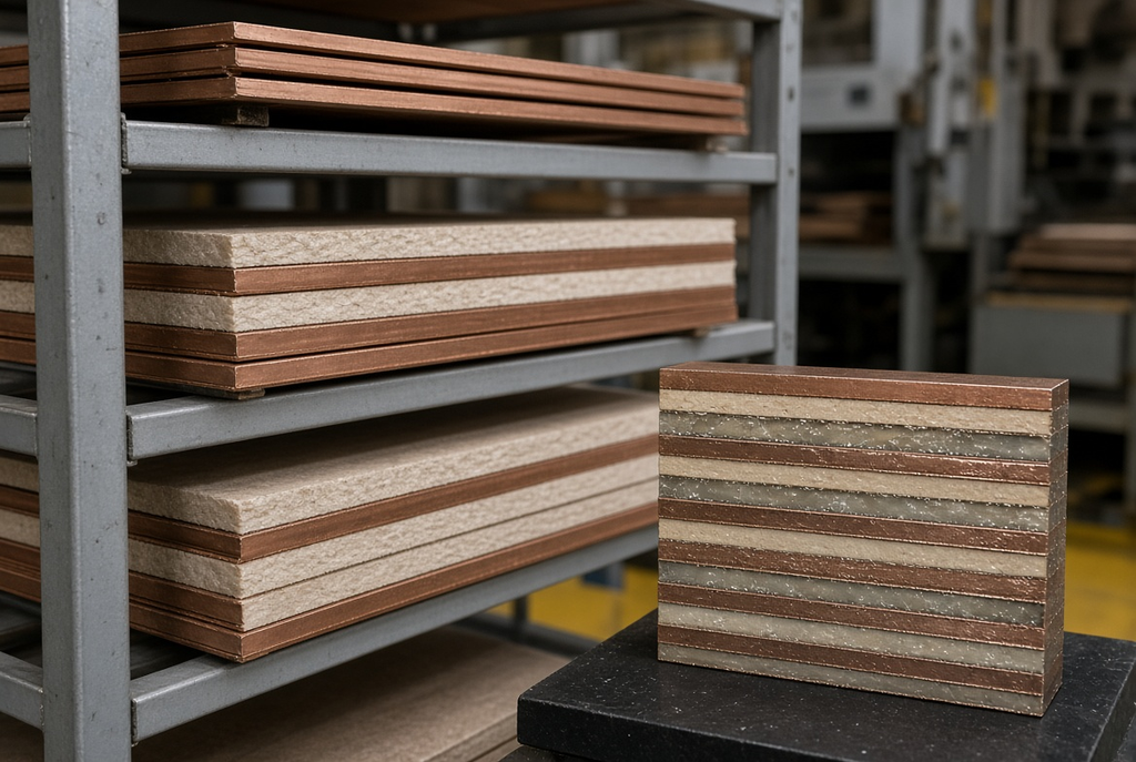
Blind, Buried, and Sequential Lamination: When Multilayer Gets More Complex
For many 4-8 layer boards, through-hole vias help to prevent lamination. That changes with blind vias, buried vias and build-up constructions. They are where the multiple layers become “more than just layers”. Use the names of the structures. A via is not a specification!
Blind and buried vias and their impact on layer transitions
A BLIND VIA is a hole that is drilled from an outer layer to one or more inner layers that will not go all the way through the board. A buried via is always connected to inner layers and does not go to an outer surface. Both of these need to be controlled depth or be drilled and plated prior to being laminated into the final board.
There is a reason why blind and buried vias lamination is a construction decision, not just a CAD via type. The factory must have information about the layers on which the hole should start and end, if the holes should be staggered or stacked, and if there should be a sub-composite that needs to be pressed, drilled and then plated before the next lamination. If each non-through hole is referred to as “a via”, then the transitions are not exposed until the process engineer has to create them.
Sequential lamination and build-up constructions
The sequential lamination PCB construction is a PCB manufacturing process which requires more than one press cycle. A sub-stack is a stack of wood that is laminated, drilled and plated. This sub-composite is then layed up with more prepreg and copper and pressed again. To add short connections between layers of a design where one through-hole drill can not reach, this build-up method is used in HDI and dense interconnect designs.
Additional pressing steps introduce more risks, more registration steps and more expense. It also adds a documentation requirement. You’re not just showing the number of layers built, you are showing the sequence in which they were built. Feasibility will be based on the design and based on the process of the fabricator. It is important not to assume that a shop that laminates a standard 8-layer construction can automatically do so with a stacked buried-via construction; it is essential that this type of construction be reviewed separately.
Common Pitfalls in Multilayer Lamination Design
As with most lamination issues, it begins with the drawing and does not necessarily begin in the press. The following patterns are frequently encountered, so if you are considering freezing artwork, be sure to look out for them.
Treating layer count as the only design parameter
“Make it 8-layer” – addresses routing density. It does not specify materials, finished thickness, copper distribution or which layers have impedance. The common symptoms which follow are unexpected warpage, an impedance reading that didn’t meet the model, and a drill that does not like the dielectric stack that the factory was forced to use. Create stack-up as a core design document, and then let the number of layers evolve from that document.
Ignoring copper balance and symmetry
Even with a clean schematic, a mechanically one-sided board can result. A panel will bow if it has heavy copper on one half only, or if there is no counter side to it. The assembly yield will decline if the board doesn’t lie flat on the stencil or fixture. Local stress is added by connectors and stiff mechanics. Designed to make a symmetrical, balanced stack (if possible, in the circuit). If a heavy-copper power layer cannot be avoided, make sure to discuss it with the fabricator prior to stack approval.
Late changes to material, thickness, or via structure
A material swap, thickness change, or last minute change from through to buried vias is not a footnote. It may result in new lamination plan, new inner-layer tooling and new qualification of impedance and thickness. Withdrawing the lock material, finished thickness and via structure prior to production release unless the change is deemed to be of value to be sacrificed in the reset. If it is worthy of the work, do it like a new construction, not a red line on the old construction.
Pre-Lamination Checklist for Multilayer Designs
Using stack-up and material confirmation prior to production.Implementing stack-up and material confirmation prior to production.
Stack-up and material confirmation before production
Verify, in writing, prior to committing to the inner layers:
- The number of layers, order of cores, prepreg and foil
- The type of material, if it affects electrical or thermal performance, and if it is a specific grade, it will be identified.
- The diameter that the finished cut should have and the allowable variation from that diameter.
- The amount of copper needed per layer
- Impedance layer and reference planes
- Flooding may occur via structures, such as through, blind, buried, stacked or staggered.
- Any special thermal or reliability requirement that should influence material/construction selection.
- If one of those is still “TBD” then the factory is still guessing. There are two ways to create the “same” board laminate differently: Guessing and cheating.
- Treating electrical, mechanical and manufacturing demands in unison
If one of those items is still “TBD,” the factory is still guessing. Guessing is how two lots of the “same” board laminate differently.
Aligning electrical, mechanical, and manufacturing requirements
Electrical performance wants controlled dielectric spacing and a stable material. Mechanical constraints want a thickness and rigidity that fit the enclosure and the connectors. Manufacturing wants constructions that match available cores, drill practice, and a cost structure the project can live with. Those three views should meet on one stack-up drawing.
Sometimes the honest answer is to simplify. Dropping an unnecessary buried via, balancing a copper-heavy layer, or accepting a slightly different dielectric thickness can raise yield without giving up function. That conversation belongs with the fabricator while the stack is still a proposal, not after the first panels come out of the press.
Frequently Asked Questions
What is the PCB lamination process in multilayer boards?
It is the manufacturing stage where imaged inner-layer cores, prepreg, and outer copper are stacked and then bonded under heat and pressure. Prepreg resin flows and cures, turning a loose book of materials into one rigid or flexible multilayer panel. After that cycle, the internal construction is fixed.
How are inner layers bonded into a single multilayer construction?
Inner layers are etched and inspected on cores first. Those cores are then interleaved with prepreg—and often with outer copper foil—according to the approved stack-up. In the press, the prepreg melts, fills, and cures, creating the dielectric bonds that hold the layers together.
Why does stack-up symmetry matter in multilayer PCBs?
A stack that is not a mirror around its centerline, or that carries very different copper density on opposite sides, expands and contracts unevenly during lamination and later reflow. The usual result is warpage, uneven thickness, and assembly problems that the netlist never predicted.
What is the difference between through, blind, and buried vias in lamination?
A through via is drilled after the full stack is bonded and passes through every layer. A blind via starts on an outer layer and stops on an inner layer. A buried via lives only between inner layers. Blind and buried structures often require extra drill, plate, and press cycles, so they must be named and layered explicitly in the data package.
How does material choice affect multilayer lamination and reliability?
Different laminates flow, fill, and cure differently in the press. They also expand differently in reflow and in service. The wrong grade—or an unspecified “equivalent”—can change thickness, impedance, via stress, and how the board behaves after soldering, even when the artwork stays the same.
What should be confirmed before releasing a multilayer design for production?
Confirm layer order, material grade if it matters, finished thickness, copper weights, impedance layers and reference planes, via architecture, and any thermal or reliability notes. Align those items across electrical, mechanical, and manufacturing reviews before inner layers are imaged. After lamination, those choices are no longer drawings.