People often ask: How to print a PCB at home, they are talking about the toner transfer or other image transfer method: print the image on special paper or film and then press it onto a copper clad board, then remove the copper from the board, and finally drill and do the rest of the board by hand. Simply could result in easy, low density boards for class lab or single experiments. It is not a fiction.
The coarse trace and the absence of controlled impedance on a home-etched board, combined with an absence of reliable solder mask and near-absence of repeatability, are all problems. Think about it as a means to observe copper become a circuit; not a means to hardware you would sell, ship, or count on in the field.
How to Print a PCB in a Hobby Context
A board is created mechanically and chemically in a workshop or classroom and the process is a short chain. Simple single-layer layout design or downloaded, printed on toner-transfer paper or transparency, heat-pressed onto cleaned copper-clad laminate, etched, rinsed and toner stripped, holes drilled for through-hole components, and a basic finish. Then a very rough mask or conformal coating is applied by some makers. It’s about understanding and not a production panel.
Where this method fits
Home etching is for learning labs, club nights or quick experiments with low voltage, low current circuits. Students will be able to explain the reasons for maintaining a continuous trace, the reason to surround a hole with copper on a pad, and the reason that dirt on copper will destroy adhesion. If a layout is wide and equipment is ready to use, a teacher can have one board run through the process in an afternoon.
It shouldn’t be on a product you’re going to sell or leave in the field. Not all the boards will be identical after a successful etch. If the circuit needs to be subjected to heat, vibration, moisture, or a customer, end here and proceed to a real fabrication file set.
Hard limits to accept from the start
The restrrictions with home-etching are revealed before the first iron is cast on the copper. The following are typical hobby results:
- Trace and space – 10s of mils – not the fine geometry a CAD default would draw.
- Lack of plated vias, or very few, a “via” is typically a wire soldered through a hole
- No Materialized Controlled Impedance and no Reliable Multi Layered Stack-up.
- No factory solder mask (any coating is hand applied and is not even)
- Rough edges, out-of-shape copper, and boards that don’t line up
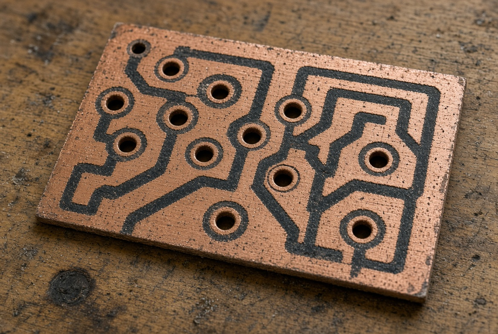
The mistake is to create a highly detailed board in CAD, then print it out and think that toner and a tray of etchant will reproduce that design. They will not. If there’s only a production density that it fits into, it’s the wrong tool.
Safety and Environmental Precautions
Please do not miss this section in order to reach the iron. The etchants that are used to etch a circuit board at home are corrosive and toxic. Copper waste, even in a small tray is dangerous. Don’t start if you are unable to protect skin and eyes, if you cannot ventilate the room and waste disposal must follow local rules.
Chemicals and personal protection
Today, the two etchants that are still commonly found in hobby shops are ferric chloride and ammonium persulfate. Both attack copper. Both splash. Ferric chloride stains and bites skin and ammonium persulfate is an oxidizer and should be avoided in organics and metal tools that you love. Fumes are not “just a shop smell.”
Use splash goggles, chemical resistant gloves and an apron. Use a chemical resistant tray, NOT a cutting board in the kitchen. Have a source of running water on hand. Work in a well-ventilated room with an open window, but in a closed bedroom with no fresh air is bad. Avoid storing etchant in food containers and never leave a tray where a child or pet can reach it.
Disposal and environmental responsibility
The copper is dissolved in used etchant and in the rinse water after the etchant. That mix doesn’t flow down your household drain. Harmless doesn’t mean there is no danger when it comes to small volume.
If supplied with instructions for neutralization, perform them according to the supplier’s instructions; otherwise, consider the liquid hazardous waste according to your city or campus guidelines. Spent etchant is collected at a household hazardous-waste collection event by many municipalities. Label the container. If everyone else does it, do not pour it on soil, into a storm drain or into a common lab sink. Clean up is part of the job; have absorbent material and plan in hand before opening the bottle.
Step 1 — Preparing the Design for Toner Transfer
The layout must be for toner and wet etching, not a factory plotter. This translates to copying the copper layer, expanding the traces and spaces, and removing the features that the process can’t support.
Mirroring and scaling
Mirror the copper artwork on the computer so that the text and connectors will be correct when transferred to the board. Print an over-layer image onto the board the “right” way around and you’ll get a reversed board. Look at the scale on the printer against a ruler and a 2 percent shrink can cause a connector to go out of place.
Extend traces and gaps wider than you would pass to the fabricator. When the toner melts and etchant undercuts the edge, the line looks good on screen, but not when it is printed. If a pad needs to have a hole drilled in it, leave a large copper ring around the hole (also known as the annular ring, which is the copper that was not drilled away). That ring, at home, is more or less. Design it to be big.
Simplifying the layout
Take off fine pitch packages, tight grids and decorative copper that cannot be resolved by the toner. Drop via farms. Use through-hole components with sincere pads. Be careful of internal corners which will trap etchant.
Never use a production Gerber set in a laser printer. The files are for plated holes, soldermask dams and etch compensation – a hobby tray can’t handle those things. Draw another teaching schematic of the circuit. This is the wrong process if the design is only available in a dense production file.
Step 2 — Toner Transfer or Alternative Image Methods
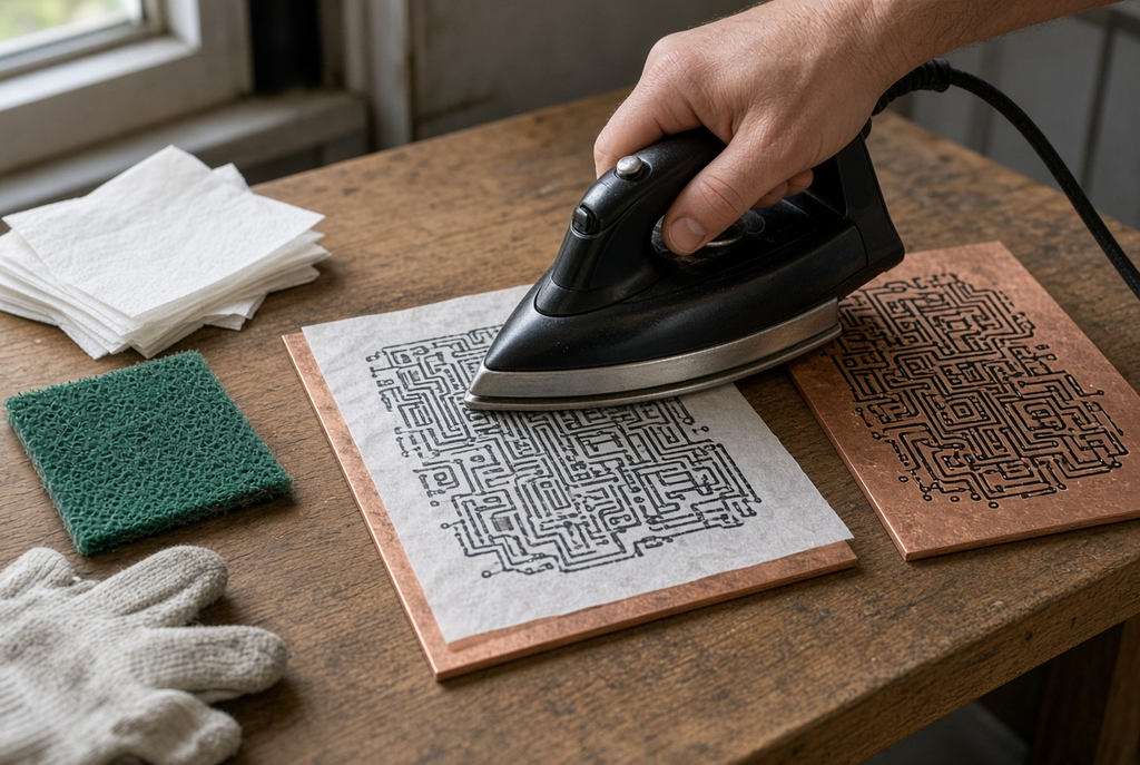
Typically, the DIY step of transferring an image to a PCB is called PCB toner transfer. Coated transfer paper or a transparency will be used for printing with laser toner which is then placed under pressure and heated onto clean copper. The toner is now used as the etch resist. The job can be done with photoresist film and UV exposure, but with a little more control, and the risks are the same, as are the etch step and its associated hazards, this article continues with toner.
Surface preparation
Make sure that the copper is cleaned and water sheets are formed rather than water beads. The three reasons for toner lifting in the tray are oxidation, fingerprints and shop oil. A fine abrasive pad, solvent wipe and then a lint-free cloth. After that, grasp the board by the sides. If the clean is skipped, you’ll be watching the traces disappear from the middle of the pad while the etch is in progress.
Heat, pressure, and alignment
The heat and pressure is provided by a clothes iron or laminator. The toner should not smudge on the copper plate. When the pressure is not even, pinholes will appear, and the etchant will go through each pinhole and undercut the trace. Take your time, you do not want to lose your paper and peel a corner of the paper to verify transfer before peeling the entire sheet.
This isn’t a double-sided board project. Home alignment is by sighting and tape. The shift level of a few mils is no longer in alignment with its hole. If two registered layers are required, do not think of it as a challenge to create a better jig, but rather as a reason to stop.
Step 3 — Etching the Board
The toning process leaves behind copper where it is supposed to be, and removes it wherever it’s not. The board is left in the etchant until the unwanted copper is dissolved, leaving the protected pattern. Watch the board. The clock is not an eyeshield.
Etchant choice and process
Ferric chloride is slow, stained and known. In the tray, ammonium persulfate is clearer and this makes it easier to see when the copper has cleared. In either case, soak the board, gently swirl to get fresh solution to the surface, and remove the board when the open copper has been removed.
Traces become fragile when left on the board “a few more minutes to be sure.” The etchant etches both horizontally and vertically. That reduces the line that you thought you had transferred. Warm solution will etch faster and more easily be overshot. A cold and tired solution deep etches forever while still producing a pink haze. Don’t make fresh chemistry for a weekend of leftovers.
Neutralizing and cleaning
Using the board lifting tongs, rinse the board thoroughly and, if the product instructions require it, neutralize the remaining etchant. Only then remove toner using a recommended solvent and/or a gentle abrasive finish. Don’t touch the wet board with bare hands. Copper salts and leftover oxidizer are still on the surface. Before making a judgment on board traces, try to dry them first as wet copper reveals nicks under a soldering iron.
Step 4 — Drilling and Basic Finishing
Make your own PCB drilling and finishing, transform an etched panel into a solderable one. Holes for through-hole leads are drilled by hand. Pads are cleanable, fluxable and tinnable. This is the complete finish. It’s not ENIG, it’s not solder mask.
Drilling limitations
Typically, a small pin vise, a hobby drill or a Dremel-style tool is the standard kit. The location of the holes is as good as your eye and bit’s wander. Copper has bits which walk on it. A hole that is at the edge of a pad leaves almost no annular ring, while a hole that makes a slice opens the net.
There is no point in fine pitch parts and vias that are too small. Etch before you drill so that you can see the pads, don’t let the board tear while drilling, and make sure that the bit does not cross the plane of the board. Before spinning the tool, if a hole must be placed between two traces where no copper is left over, then redesign the pad.
Simple finish options
If soldering to the remaining copper pads, use a soldering iron and flux to tin the pads. There are some makers that paint a conformal coating over the finished board as a very rough approximation of mask. This film can prevent fingerprints from sticking to copper. It is not a factory solder mask, it does not specify any pad openings, and it does not make the board suitable for the wave or reflow production.
Please don’t sand the traces thin to get them “professional.” They will be shattered.
When to Stop Using Home-Etched Boards
There is no quality argument for toner transfer vs professional PCB work. It is a use contest. Home-etched boards help process and demonstrate a sketch. They don’t transport a product.
Signs you have outgrown the method
To stop etching at home, if the following occurs:
- The circuit operates at a higher frequency or current than a wide and uneven trace can possibly deliver.
- There should be controlled impedance, defined stack up or more than one reliable layer in the design.
- You want to send or sell the equipment
- Matching boards, revision control or a finish that will withstand assembly heat are required.
- The only evidence of reliability you have is “It worked once.”
Continuing because the first board lit an LED is how a classroom method turns into a field failure.
Moving to professional fabrication
When the schematic is stable and the layout needs real geometry, the next step is professional PCB fabrication with Gerber data, a defined stack-up, and a specified finish. A manufacturing partner such as CKS Circuits—a Guangdong PCB and PCBA company that reviews fabrication data before production—belongs in that later stage. Home etching is not a stepping stone into that workflow, and it is not a substitute for it.
Common Mistakes and Failure Modes
Most ruined boards fail for one of three reasons: the toner never bonded, the etch ran too long, or the drill removed the copper the pad needed.
Traces lifted by poor adhesion
Oil, oxide, or weak heat leaves toner sitting on the copper instead of fused to it. In the tray the resist lifts in flakes. Etchant rushes into the gap and opens the net. If toner peels with the paper in long strips, stop and reclean. Do not “spot fix” a hole in the resist with a marker and hope the etch respects it.
Over-etched, weak traces
A board left in ferric chloride until “all the pink is gone” often loses the edges of every trace on the way. The line that survives is narrower than the artwork and fragile at bends. Pull the board when the field copper clears, rinse immediately, and inspect under good light before you strip the toner.
Misaligned or broken holes
A walked bit cuts the pad into a crescent or breaks into a neighboring trace. Assembly then depends on a sliver of copper. If the remaining ring is a sliver, abandon the hole and decide whether the board is still a teaching piece. Forcing a header through a damaged pad usually lifts the rest of the copper.
A Simple Decision Checklist
Use this list before you mix etchant, and again before you etch a second revision.
- Is this for learning or a one-off experiment, not a product you will ship or sell?
- Are the traces wide, the parts through-hole or very coarse SMD, and the layout single-sided and sparse?
- Do you have gloves, eye protection, ventilation, and a legal way to dispose of copper waste?
- Can you accept rough edges, hand-drilled holes, and boards that will not match each other?
- If the answer to any production, safety, or complexity question is no, the board should be fabricated, not printed at home.