Most of the people who ask the question why are circuit boards green are looking for a hidden chemistry rule. Practical would be simpler. Green solder mask was adopted as the industry standard because the imaging process has been well developed, operators can use it to check against it and the pigment was standardized by the material suppliers. The color is not vital to the board. The solder mask is — thin insulating film, which covers the copper, leaves pads free to solder, and minimizes bridges during assembly.
Green is not mandatory, it’s a default. Electrical performances don’t necessarily get better when you change colors. Use the mask as a fabrication feature and then specify it, along with the rest of the board. If the board has to be fabricated from Gerber and a fabrication drawing, begin with PCB fabrication.
What Solder Mask Actually Does
Take a complete bare board to a light table and the first layer is green. The polymer film is placed over the outer copper and then imaged and developed, leaving pads and test points, etc. exposed for soldering. That film is called solder mask. Not the metal or organic covering on the open copper. The surface finish is the second coating – and the combination of the two gets people into trouble with each other when discussing “gold boards”, but they’re thinking of a different mask color.
It’s easy to mix up the function and the color of solder mask. The purpose of the function is to provide insulation, protection, and control of the surface to which solder may wet. The pigment is what you can take photos of.
Protection and assembly aid
Mask is completing three mundane tasks simultaneously on an assembly line.
Firstly, it prevents solder from spreading over the copper which is designed to remain unsoldered. Due to the close proximity of neighboring pads on a fine pitch footprint, there is the potential of a slight over deposit of paste-to create a bridge. That risk can be lowered with a well-registered mask dam between those pads. The dam does not address a correct stencil aperture or controlled paste volume. It provides an actual stop to the process, making a small error less likely to be a short.
Second, it is used for traces and plane copper which would be left exposed to handling, moisture and shop air. Uncovered copper oxidizes. It also scratches. A nice CAM trace can get picked up a nick on a panel edge or rack finger before the board even gets to the paste. Mask will not make a fine line stronger electrically, but will shield that copper from being a handling problem.
Thirdly, it gives the outer surface uniform texture for the printing of paste and component positioning. Paste requires a well-defined pad, not a smeared-out copper pad that extends below the edge of the mask. The printer is able to view the same target from board to board as long as the opening is clean and the mask is completely cured.
One often made error is using the mask as a substitute for a good finish on pads that require soldering. The mask is used to protect the copper that it covers. It does not terminate the open copper. These remain exposed pads require HASL or ENIG or other mutually agreed upon finishes to allow for solder wetting after storage and after reflow heat.
Mask openings and pads
Many times a mask layer’s useful component is the hole it contains. CAM engineers spend real time opening the PCB mask over pads: Size of the pad opening compared to the copper pad (solder-mask defined versus non-solder-mask defined), the amount of clearance around a via, and if a test point appears open in the layout but covered in the Gerber.
The opening affects the solder joint. A narrow opening may result in a starved joint or may leave a mask lip that the paste will not reach. An oversized opening will allow solder to run over the pad into nearby copper or into a via. In neither problem, does it appear as a “wrong color.” Both appear as a failure of the joint to pass inspection or as a failure in the field.
The other fault type is easier, and more embarrassing. The pad is laid out correctly, a designer planned to allow soldering, and the mask layer during the fabrication process still covers the pad. The board is returned ready for use. Parts cannot be placed on a pad that’s not there. That is always easier to catch in a CAM review than after paste is down.
If you are making your own pad and mask data to send to a fabricator who can use it, follow the pad design guidelines for clearance, pad opening and pad preparation rules, don’t create your own in the notes field.
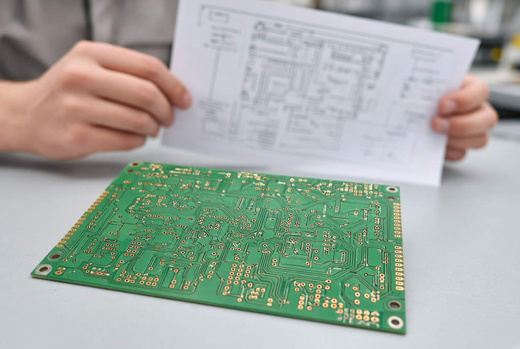
Why Are Circuit Boards Green: Process and Supply Chain
It is not true that green won due to its electrical superiority. It won because early liquid photoimageable masks had green pigment that was easily imaged, reliably cured, and was a color that an inspector could work with all day. The equipment, chemistry, and training were developed around this selection. When a process window is that mature, shops continue to use it, unless a project provides them with a reason to not do so.
Process maturity and inspection
Speak to an AOI programmer or a visual inspector about their preferences of which boards they would rather debug at 2 a.m. The majority will point to GREEN. Green solder mask falls within a contrast range that facilitates the visualization of traces, pad edges, exposed copper and missing-mask defects. Solder bridges will appear as bright metal on the green field. Any gaps in the mask will appear as “unexpected copper. When white, Silkscreen is easy to read.
Dark colours absorb more light. Black mask is especially useful at concealing a hairline bridge or thin strip of exposed copper until the board is under a different angle or a different camera setting. That doesn’t make black “bad. It involves a change in the recipe of inspection that must occur as the color changes—and some person must be responsible for that change before the first panel reaches the line.
The colour of the solder mask can make a difference to the inspection, and that’s part of the reason buyers choose a colour from a catalog photo. Deciding on a colour that is more difficult to detect defects, followed by an argument about escapes at assembly – is a process issue arising at the specification stage.
Supply-chain inertia
Once green became widely used, a number of laminate shops and suppliers of masks, fabricators and assembly houses stocked and qualified around it. The standard color is already available. Process window is already defined. Incoming inspection has an idea of what good looks like.
A non-green mask is another material lot. This might require an alternate exposure energy, develop time or cure profile. There are some stores that have those colors available each week. Others consider them a special process and make a different day for them. The common error is to use a nonstandard color as free. No changes were made to the electrical stack-up. The material and scheduling window of the shop did.
This is no justification for excluding other colors. It asks the question: “Is it worth another process step to get the color to do work?
When Other Mask Colors Are Used
Real products appear colored black, blue, red, white and other colors every day. For using the non-green PCB mask, it is not a performance competition. Insulation value of mask is unchanged by pigment. What modifications are required for branding, contrast for assembly and inspection, and how easily can the legend be read by the operator.
Branding and product identity
Colours are often used as identity when the hardware is for consumers or limited editions, or the boards are placed visible in a clear or open enclosure. The black board that is behind a smoked window appears complete. A display unit with a red board is equivalent to a brand panel. As a valid excuse to go green is a good one.
The problem is selecting the colour at a marketing conference and finding it difficult to see the solder connections in the finished product or the white legend showing through on a light mask. Brand identity should be on the enclosure and the silkscreen, just as it is on the mask. If the board will not be seen, the color is decoration paid in process attention.
Assembly and optical considerations
Machine vision won’t say “pretty. It sees contrast. Some colours absorb illuminators and some reflect illuminators. Solder balls and thin solder bridges can be hidden in dark masks. The next time they choose to wear a very light mask, the white legend will be washed out, and polarity marks will be more difficult to read. No assembler will get the same first pass on black that they did on green without making some adjustments to the lights, thresholds and sometimes the camera angle.
When a product requires a non-green mask, communicate this to the assembly and inspection teams before the first article and not after the first escape! Colour remains a fabrication call. It also serves as an input for assembling.
Mask Color vs Surface Finish
Both of these layers are located on the outside of the board and both are shown on the fabrication drawing; that’s why they are mixed together. They are not interchangeable with each other.
Color of mask is pigment in the insulating film. Surface finish – the metal or organic coating on the copper that the mask left open – HASL, ENIG, OSP, etc. The finish determines its solderability, shelf life and its performance in reflow. The colour of the mask is not.
The board may be green and have ENIG pads. May be black with HASL pads. A HASL pad does not change when changing from green to blue mask. Surface finish vs solder mask color is the difference that maintains an accurate quote.
Choosing finish before color
Secure the end against the assembly and storage window and against the reliability need. Typically the discussion of the finish is stimulated by fine-pitch, a number of reflows, or the long shelf time before assembly. Mask color may be delayed until the color is more stable after the decision was made, provided that the fabricator can get the color to run on that construction.
The opposite of this is a compromise that is unnecessary: selecting a color for a photo and then having to squeeze the finish to what’s left on the same traveler. Finish first. Color second. Both should be marked on the drawing: Notes on the drawing should be first, then both.
Practical Guidance on Specifying Mask Color
Color of solder mask should be selected after stack-up, material, surface finish and pad geometry in fabrication. Colour is a secondary call. Do not take the first cycle of review to get the pigment correct, because the openings over the pads remain incorrect.
Questions to ask before choosing a color
Double check whether the color is essential or not. Green is the least surprising color when the board is not likely to be photographed for a product page, and is housed in a built-in opaque container.
Check that the fabricator will be able to provide the color on this construction and if it will affect the lot timing. The color that is standard on a two-layer consumer board might be special on a thicker multi-layer panel.
Question on how the colour will appear under AOI and visual inspection and if the legend colour still contrasts. The combination of white and green is a combination that is known. Reading on white or yellow mask is a white legend.
Is the first construction a small model? There should only be a custom color when it is necessary and useful, and not for cosmetic reasons.
Record the answer in the fabrication notes under the color and finish not the mood. Green mask, ENIG is a specification. No, “make it look premium” is not.
If CKS Circuits is looking at the package, then the relevant conversation is the one prior to manufacture: Gerber upload / mask openings / finish / drawing notes. Colour may form part of that review. It shouldn’t be a part that slows down the current carrying parts of the board.