A completed bare circuit board doesn’t result from sending a Gerbers zip. Once a PCB fabrication package is ready for the approval stage and is complete enough to be tooled (current revision, stack-up, copper, drill, outline, mask, finish and the checks required to release it), a controlled sequence is followed in the factory that builds the PCB. Typical reasons for engineering questions to halt the job before cutting laminate are the absence of drill files, undefined thickness, conflicting finish notes and the lack of a side message test expectation.
Gerbers are not the sole solution. The factory will not “just figure out” the number of layers, materials, via intent, and which file wins if the drawing and the image disagree. The decisions should be in your package, not a conversation that never gets to the traveler.
A Finished PCB Is a Bare Board, Not an Assembled Product
For the purpose of this article “finished” shall mean a fabricated bare board delivered to the approved fabrication package. Does not imply sourcing, placement, reflow or functional test. That boundary is important because sometimes purchasers put only Gerbers to the fabricator and expect him to turn them into an assembled product, and other times they put a bare-board order along with a BOM and a centroid file in it and ask why the fabricator is asking for copper weight rather than part substitution.
What a bare-board traveler cares about
The bare board traveler follows construction and image, rather than placement. It is concerned with stack-up, drill, copper, mask openings, surface finish, outline and electrical continuity compared to the manufacturing netlist. An assembly traveler is interested in BOM, centroid, polarity, paste and placements. On a fabrication only order, if the person who ordered asks “why are you asking about my BOM?” – The two jobs have been mixed. If a person thinks that functional testing is due on a board with no components on it, then it will also appear like that.
Why confusing bare board and PCBA creates wrong questions
That combination leads to the wrong quotation, the wrong file request and engineering questions that should not have been asked. If a fabricator has not been provided with an intent to stack, finish and test in an assembly file, he must create these himself. The later sections of the data package, process stages, and release checks are usable rather than abstract because they use the understanding of the boundary.
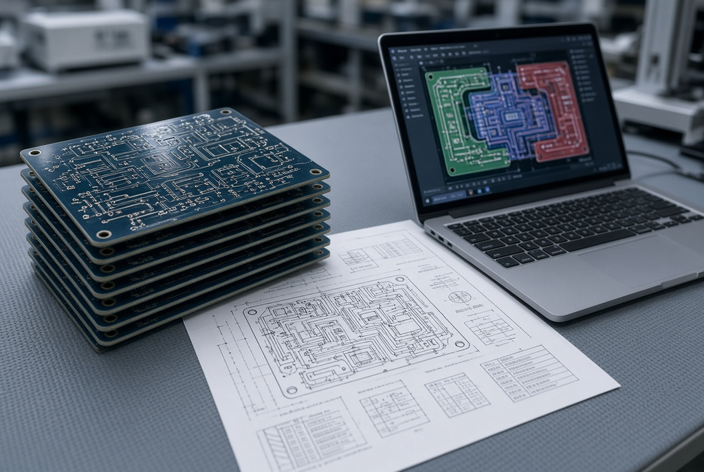
The PCB Manufacturing Process Starts With a Complete Data Package
Fabrication has not begun until a zip file has arrived. It begins with the fabricator understanding what revision they are working with and what the copper, holes, outline, materials, thickness, finish and special requirements are. One set of Gerber layers is usually not the complete layers set. The most common reason for a PCB fabrication process to stall in engineering rather than progressing to material issue is that set is incomplete.
Copper, drill, and outline data have to agree
The image to be imaged and etched are defined by copper layers. Drill and rout data are used to create holes, slots and mechanical path. The outline is used to specify the final geometry of the board. These three families need to give the identical description of the board. A small omission that is called out on the drawing but not in the NC drill file is not a small omission, it’s a tooling conflict! A routed feature, which is drawn only on a copper layer, is of the same class of problem. The data package for PCB manufacturing must contain such features openly rather than graphically.
The drawing and stack-up carry the decisions the image cannot show
Gerbers show geometry. They are not purposeful. Normally the finished thickness, material, copper weight, surface finish, mask color, impedance notes, critical dimensions, and special via requirements are included in the fabrication drawing or in the stack-up. A file with different finish names, or a traveler with layer names and no construction to build will leave the traveler unbuilt. Write the answer in the box. Don’t assume that the fabricator will use a “standard” answer that will fit your design.
What the fabrication package should define
| Define in the package | Do not leave for the fabricator to guess |
| Current revision and which file wins if data conflicts | A folder of mixed exports with no revision note |
| Layer count, stack-up, material, and finished thickness | “Standard multilayer” with no construction |
| Copper weight and any impedance requirements | Trace geometry with no impedance target or reference layers |
| Drill, slot, and via requirements, including filled or special vias if needed | Holes drawn only as graphics |
| Solder mask, legend, surface finish, and outline | An assumption that color, finish, or profiling is always the same |
| Test, panel, marking, or other special instructions | A note in an email that never enters the fabrication package |
CAM and DFM Review Happens Before Material Is Cut
The delay isn’t CAM. It’s where the factory verifies if the data can be tooled: layer alignment, drill-to-copper relationships, clearances, mask openings, missing files and conflicts between the image and the drawing. PCB and DFM review is at the point and time for questioning risks before laminate is issued, not after boards are completed.
Return questions tend to be specific. Which note is now? Does this hole include a plating? Is the stack-up determined or proposed? Are the impedance values prescribed design targets or verification values? Provide answers to those questions in the data package. A reply that is in a chat thread will not be sent with the job. Clearances, annular ring, drill size and others are subject to design, and the current capability of the fabricator, not from a previous vendor or previous revision.
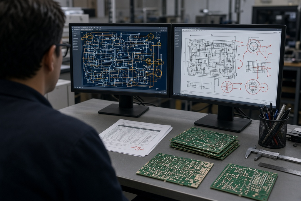
The Factory Sequence Follows the Construction, Not the CAD Layer Order
Shop order is based on the order of the board as it is built, not the order of the layers in CAD. In a multi-layer board, further layers are imaged, etched and checked prior to pressing. The sequence is not the drilling of a through-hole before the exit of the stack. A simpler double-sided board eliminates the inner-layer and press stages. Blind, buried, or sequential constructions add steps and should be included in the data, not found on the floor.
Inner layers are imaged, etched, and inspected before press
The technique of photo-imaging is used to transfer the inner copper pattern onto the core. The unwanted copper is removed by the Etch. Before burying this image, it is checked by inspection. The reason is that the defect is located at the bottom of the stack, making it harder to recover than an error at the outside of the stack. The inner-layer registration or etch quality could be incorrect, and the fault is fixed in the stack in the press.
Lamination locks the stack-up
Press cores, prepreg and copper into construction as described in the drawing. At this stage, registration, finished thickness, copper balance and symmetry are important. Sequential or HDI-style builds alter the path and add steps to the process, and are not a default traveler. If it’s just a list of layer names, the factory is not able to lock a construction it was not given.
Drilling and metallization create the layer connections
Plated holes join layers together by mechanical drilling, hole preparation and copper plating. There, the path will be different because of laser or sequential via structures, and the path should be clear in the package. If the drawing doesn’t specify plated, filled or backdrilled then all holes are considered “a via.” Note: Intent of hole is not informal language, but drill data and notes.
Outer layers, mask, legend, finish, and profile complete the bare board
The rest of the copper is defined by outer-layer imaging and etch. Solderable openings are specified using solder mask. The board is marked with legend. Surface finish prevents the copper from oxidizing prior to soldering. Profiling or scoring will cut the outline that it is sent. One of the tasks for each step. Two “approved” boards leave the line different ways: choosing a finish, mask color, or panel method after the traveler has already been built from another note. The same decisions must be made and remain in the package until the multilayer PCB fabrication steps after the press are completed.
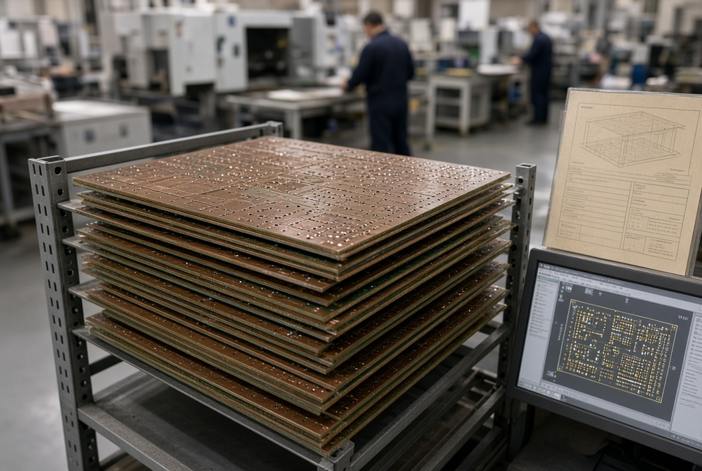
Release Depends on the Checks Agreed for That Board
A board isn’t finished if it’s ‘full’. The release is dependent upon the inspection and test plan agreed on that design and order. At overview level that plan can encompass visual inspection, dimensional check and electrical open and short circuit testing. If requested by the design or purchase order, an impedance verification, microsection, or other analysis may be required. Not every job will automatically be part of their workflow.
Bare-board electrical test: continuity vs. the manufacturing netlist. Does not guarantee the working of an assembled circuit. Not all orders include the AOI, flying probe, fixture test, impedance coupons or microsection. Before traveler is released, write the appropriate checks into the package.
Cost, Yield, and Schedule Are Set by Construction and Clarity
Layer count, board size, material availability, copper weight, via structure, impedance control, finish, panel method, and test requirements change the traveler. A clean four-layer board with a defined stack-up is a different job from a sequential or impedance-controlled build with incomplete notes. The PCB fabrication workflow follows those variables, not a generic “standard board” price.
Chasing a faster slot by leaving finish, thickness, or drill intent undefined usually costs the time you thought you saved. The files go in quickly. Engineering questions come back. Material stays unissued until someone decides which note is current. Clarity at submission is faster than optimism.
A Pre-Release Checklist for the Next Fabrication Order
Verify: before you send next package from Gerber files to finished PCB:
- Fill in copper, drill, slot and outline information that are consistent and compatible
- The thickness, material and required amount of copper for stack-up is determined.
- Solder mask, legend, surface finish and critical dimensions
- Special via or impedance notes, including those as requirements instead of assumptions
- The anticipated outcome from the inspection or test.
A common practice to rebuild the traveler after the job is running is to approve a quote at one revision and to send the next revision to production. Use the same package that you’ve quoted.
Frequently Asked Questions
What files start the PCB manufacturing process?
A usable start is not a single Gerber folder, but a fabrication package. Typically, it is copper layers, the drill and rout data, the outline, the fabrication drawing, the stack-up and notes for mask, finish, and any special via or test notes. File names depend on the CAD program used. The fore-mentioned decisions do not.
Are Gerber files enough to fabricate a board?
Not by themselves. Describe the picture using a few Gerbers. They are not consistently revision controlled, finished thickness, material, copper weight, intent (plated versus unplated hole), finish or test plan controlled. They must be specified on some part of the path where the traveller can find them.
What is the difference between a finished bare PCB and a PCBA?
A fabricated board delivered against the fabrication package that has no components installed. A PCBA is a board once components have been placed and soldered into an assembly package. Net testing of electrical on bare board. Not a substitute for functional test of an assembled product.
Why does a fabricator ask questions before production?
CAM/DFM review is less expensive than cutting the wrong stack. Typically, the image, drawing and notes will not refer to one board when questions are present. By answering them in the package, one does not have to repeat the question in the next revision.
Does every PCB go through the same process steps?
No. A double-sided board is not pressed and has the inner layers different from a multilayer board. Steps are added for blind, buried or sequential constructions. The walker does not walk one shopping tour but the one which you have defined the construction as.
What should be confirmed before the board is released?
To ensure the correct revision is built, the inspection and electrical-test plan agreed upon in the order, and additional checks called for on the drawing or purchase order. If it was not written down, it is just a guess that it is “released”.