
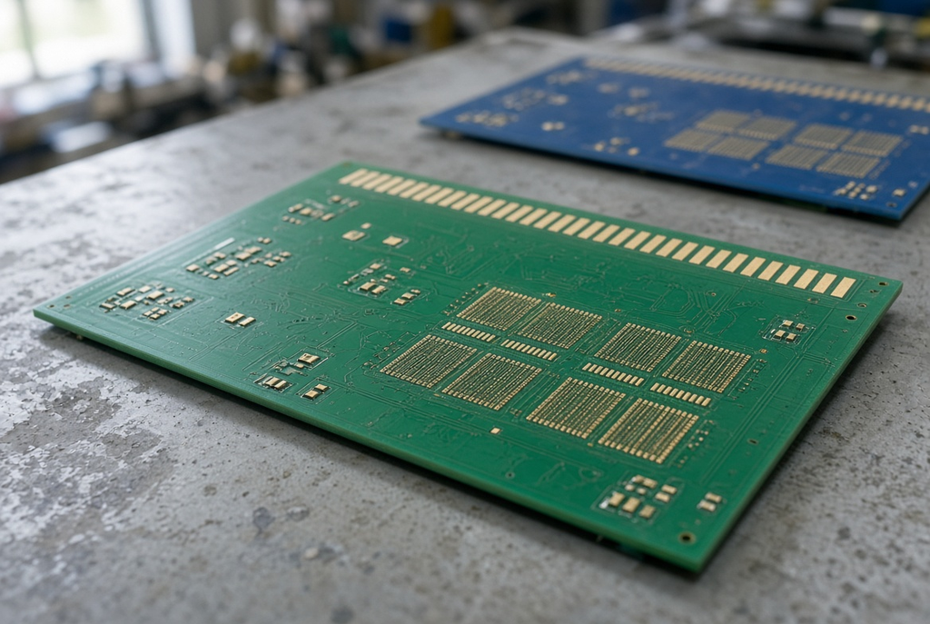
PCB Solder Mask: Types, Colors, Materials, and Design Guidelines
This guide is for PCB designers, NPI engineers, and hardware teams who mix up solder mask with silkscreen or surface finish. It explains what the mask actually does, how LPI and specialty systems differ, what color changes versus what it does not, and which openings, dams, and via treatments to lock before you release fabrication data.
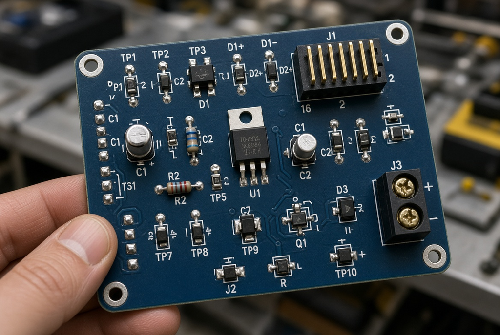
PCB Silkscreen Explained: Purpose, Design Rules, and Common Mistakes
This guide is for PCB designers, NPI engineers, and hardware teams who treat silkscreen as leftover artwork. It separates decorative text from a functional PCB legend layer used in assembly, test, and field service. You will leave with practical decisions on reference designators, polarity marks, clearance to pads, and what to check before releasing fabrication data.
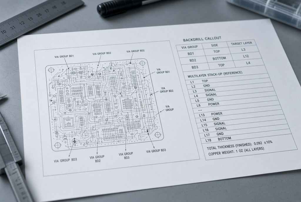
PCB Backdrilling Explained: Stub Removal, Design Rules, and Applications
High-speed PCB designers, NPI engineers, and hardware teams use this guide to separate useful backdrilling from habit. It explains how via stubs form in multilayer stacks, when residual stub and drill tolerance matter, and what the fabrication package must state—vias, side, depth, and keep-out—before a high-speed design is released.
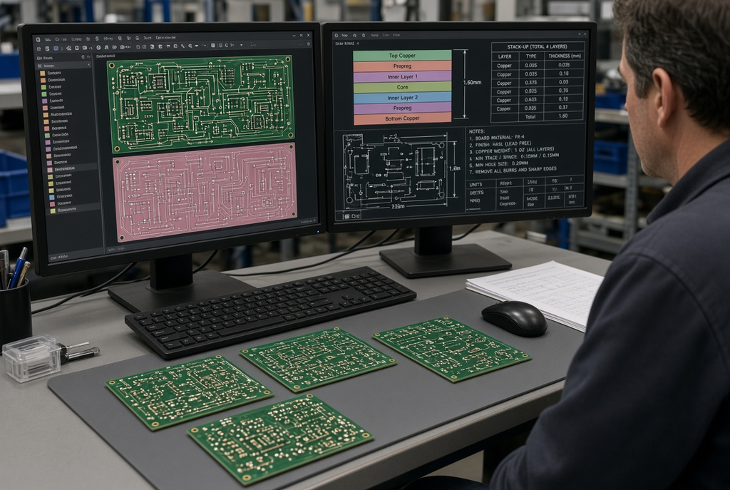
Rapid PCB Prototyping: How to Prepare Design Files and Avoid Production Delays
This guide is written for PCB designers, NPI engineers, and hardware teams who need a fast first article without an engineering hold. It separates exported Gerbers from a production-ready data package, then walks through drill, stack-up, finish, revision, and DFM checks to complete before you request a rapid prototype build.
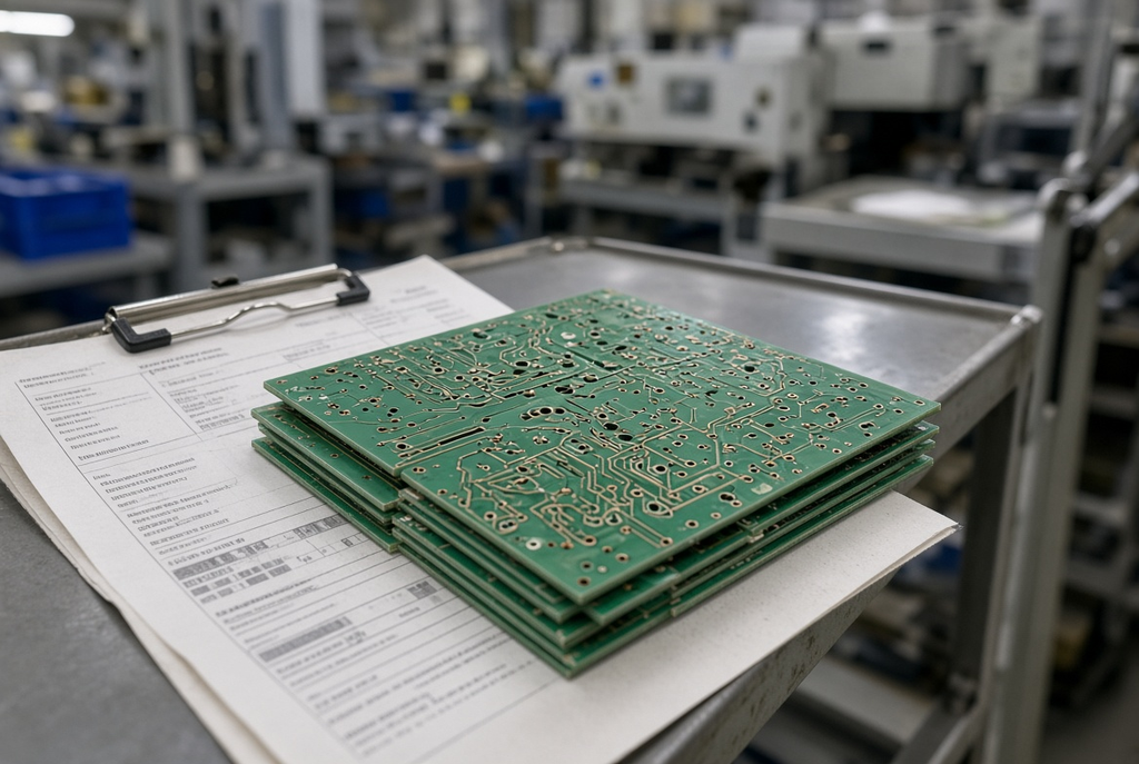
What Is Quick-Turn PCB Manufacturing? Lead Times, Requirements, and Trade-Offs
This guide is for PCB designers, NPI engineers, and sourcing staff deciding whether a prototype, revision, or small batch belongs in an expedited slot. It explains what quick turn changes on the shop floor, which files and construction choices support a realistic PCB prototype lead time, and which cost, review, and production trade-offs to settle before requesting expedited fabrication.
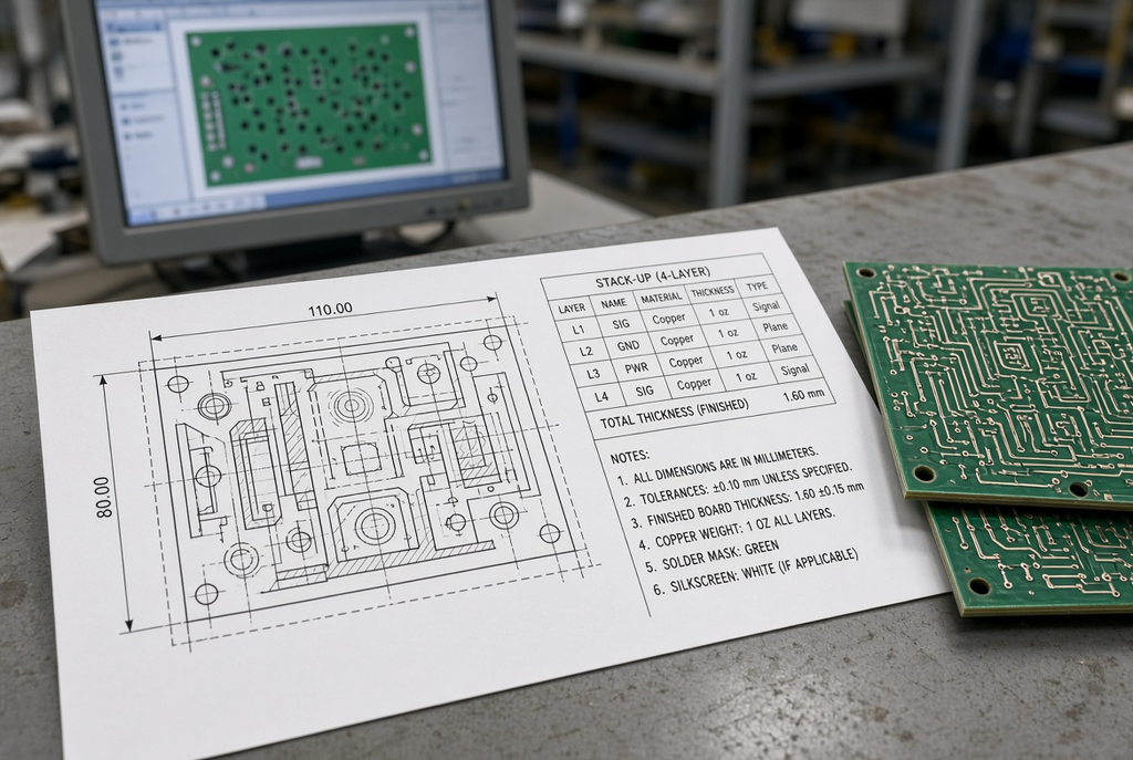
PCB Fabrication Drawings: What to Include for Accurate Manufacturing
A practical guide for PCB designers, NPI engineers, and sourcing staff on what belongs in a PCB fabrication drawing. It separates Gerber geometry from fabrication intent and shows how to define revision, stack-up, thickness, finish, vias, and impedance so bare boards are built from one controlled package.
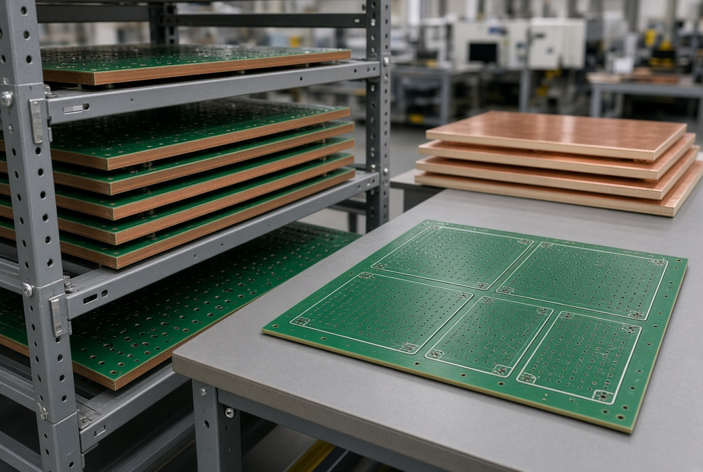
Standard PCB Panel Sizes: How Fabricators Plan Production Panels
This guide is for PCB designers, NPI engineers, and sourcing staff who have been told there is a “standard” panel size and then seen quotes that do not match that assumption. It explains why customer delivery panels and fabricator production panels are different objects, how laminate, equipment, and utilization drive panel planning, and which outline and quantity decisions to lock before fabrication data is released.
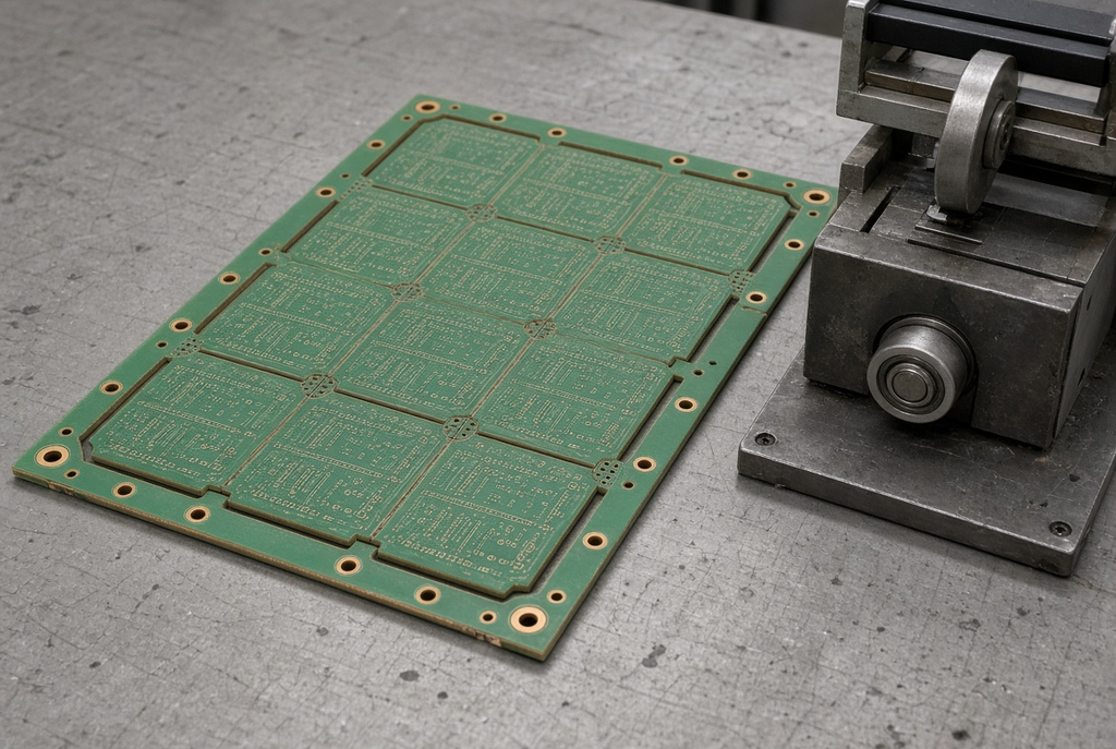
PCB Panelization Explained: V-Scoring, Tab Routing, and Design Rules
A practical panelization guide for PCB designers, NPI engineers, and hardware teams who need to choose V-scoring or tab routing before releasing fabrication and assembly data. It explains rails, fiducials, keep-outs, and depaneling so the array survives SMT and separates without cracked boards or damaged edge parts.