PCB Trace Width vs Current: How to Size Traces for Current and Temperature Rise
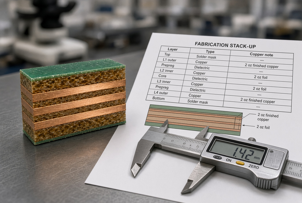
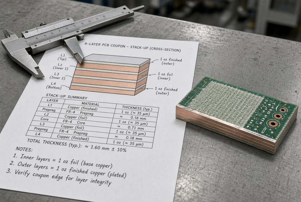
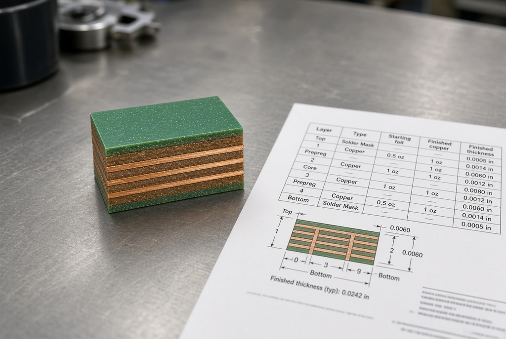
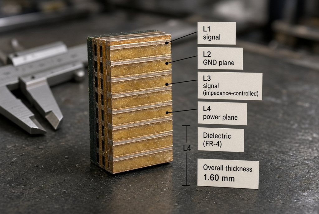
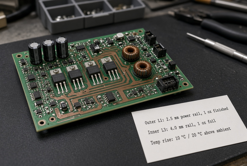
This guide is for PCB designers, hardware engineers, and layout engineers who need to size traces for current without treating a calculator result as a finished spec. It explains how copper weight, inner versus outer layers, allowable temperature rise, and etch change current capacity, voltage drop, and cost, and how to write those choices so fabrication does not guess.