The PCB stack-up is composed of signal layers, plane layers, dielectrics, copper weights, laminate materials and defines the stack up impedance, return paths, noise coupling, thermal properties, and warpage. It’s not about how many layers a PCB needs. It is the construction that allows to meet signal-integrity and power-integrity goals while building a board that is also available to build from first articles to repeat production.
A stack can generally be “locked” when a team has decided on how many layers and how thick of a stack they want. This leaves reference plane positioning, thickness of the material, copper balance and class of material as secondary concerns. These decisions will determine whether the impedance controlled nets will go on track, keep the power line quiet or keep the board flat on the table when laminated and assembled.
Defining the Layer Strategy: Signal, Plane, and Power Layers
Before adding numbered layers, decide on what each layer will be used for. A Limited Set of Routing and Reference Resources is called a Multilayer Board. All these are competing for the resources of high speed nets, analog islands, several power domains, and thick BGA fanout. If you are going to use thicker layers then you only add in costs and bulk and you are not addressing the electrical problem that caused the stack in the first place.
How Many Layers Are Actually Needed?
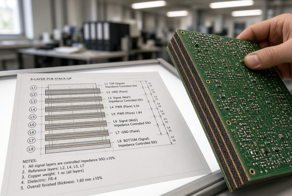
First of all, identify the number of high-speed nets that need controlled impedance, the number of independent power domains and the quality of the return path needed near to those nets. If the bulk of routing is on the outer layers, and if you can return to one solid ground plane and get power from another solid ground plane, a 4-layer board might be sufficient. If there are more than two layers of signals which need to be adjacent to a solid plane or if there are more than two rails that need to be a particular copper type then 6, or 8 layers, are reasonable.
If only “extra copper”, adding more layers is seldom a good idea for signal integrity. If the analog net is sensitive, a noisy digital bus can be added if a missing reference is present, and if the high current rail it requires a missing reference, additional layers can be added without the need for all of the high current returns to pass through a broken plane. If there is a sign or a power utilization that can’t be called, a new layer will do and it will be a cost without benefit.
Assigning Signal and Plane Layers for Clean Return Paths
The number of layers is only about the number of copper foils you have. Those dielectrics between those foils set up the impedance, coupling, loss and the board’s reflow behavior. This should be a conversation that includes both the class of material and the core/prepreg construction; it should not be an “afterwards” e-mail for materials.
First of all, core, prepreg and material classes.Selection of the core, prepreg and material class is the first one.
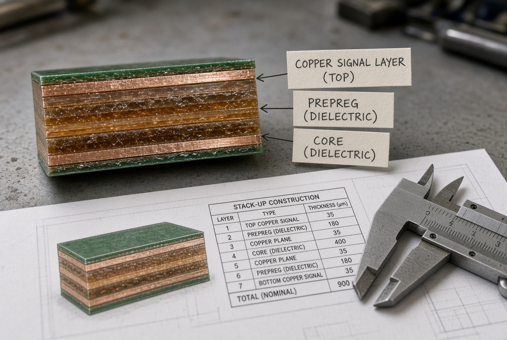
The cores are constructed of copper and the prepreg are sandwiched in between and lamination preforms the filling and bonding of the stack. A core consists of a known and stable dielectric between two copper foils. Prepreg flows, fills and sets the spacing between cores and a core and outer foil. The combination you want to use should be a part of the construction and not around the layer list.
Materials and Dielectric Choices in the Stack
The number of layers only indicates the amount of copper foils you have. Those dielectrics determined the impedance, coupling, loss and the behavior of the board during reflow. The assignment of material should be discussed with core/prepreg construction, and not be separated into a different “materials later” e-mail.
Core, Prepreg, and Material Class Selection
The prepreg sheets and copper-clad cores are stacked, and the prepreg layers fill and fuse the stack during lamination, forming a multilayer stack. Cores provide a known and stable dielectric between two copper foils. Prepreg flows, fills and sets cores and spacers between cores and between core and outer foil. You are not decorating around the layer list, you’re putting the combination you choose together.
The materials class comes after the requirement of thermal, electrical and reliability. For many commercial and industrial boards that are not subjected to high speed loss or high assembly temperatures, standard FR-4 is the default. If the board will be reflowed more than once, is a thick board or has a high operating temperature, then high-Tg materials may be a more suitable starting material. When insertion loss or fast, long nets with a requirement for dielectric constant control are the limiting factor, then low-loss or high-frequency laminates enter into the discussion. Match classes with the jobs. Unless there is a reason why one needs to specify a specialty resin system “because it sounds better”, it is generally a cost and availability risk.
Don’t include brand names or unqualified fabricator capability lists on the drawing until the fabricator verifies what he or she has on hand and can qualify. The drawing should make an electrical and thermal statement. The construction should be selected from the constructions that can be repeated by the shop.
Dielectric Thickness and Its Impact on Impedance and Coupling
The primary geometric lever of a signal layer and a reference plane in a PCB stack-up is the dielectric thickness. Thinner dielectric reduces the impedance of a trace of a given width, while increasing the coupling to the reference, which is beneficial for a controlled impedance routing and for minimizing the area of the loop. It also brings the noisy net on one layer closer to a victim layer on the next layer, thus enhancing layer-to-layer coupling.
Very thin dielectrics are useful when a small trace width requires 50 Ω or 100 Ω differential, or when a tight power-ground sandwich is desired for power integrity. They also increase the sensitivity of the stack to the presence of resin, thickness differences in the press, and roughness of the foil. Thick dielectrics have the opposite effect: They make it more challenging to hit the target impedances with narrow traces and they make the reference more difficult to hit, increasing inductance and crosstalk. Once you have selected the thickness for the impedance and coupling, ask the fabricator what core and prepreg combinations they can maintain in production.
Copper Weight, Balance, and Symmetry
Copper is an electrical conductor and a mechanical layer of the laminate. The current capacity, etch geometry, impedance and warpage after press and reflow are the factors that are influenced by weight, distribution and symmetry.
Choosing Copper Weight for Power and Signal Layers
Outer and inner copper weights are selected not from a default. A thicker copper power plane and/or a higher current carrying inner layer will increase ampacity and reduce the DC drop. Etching is more difficult with the same heavy copper on a fine pitch signal layer and the geometry of the trace is not the same as that used by the impedance models. Don’t have to match the inner and outer copper. Many boards employ lighter foil on impedance controlled layers of signals and heavier foil on power planes.
A power rail with copper in excess should be a dedicated plane or a wider pour with all signal layers the same heavy weight. If heavy copper and fine traces are to be mixed, file an early record of that. The fabricator requires it for etch compensation and as part of a standard process or special build.
Copper Balance and Warpage Control
In the manufacturing of PCBs, the copper balance and warpage occur after lamination and after assembly. A stack containing heavy and large copper area on one side and light, sparse copper on the other side is pulled during cool down. The board bows. Then there is the issue of assembly which stresses plated holes and solder joints, and thermal cycling can further challenge the same areas.
Wherever possible in the electrical design, aim to achieve symmetric copper distribution around the centre line of the stack. Use mirror plane layers, not have all the heavy copper at the bottom half of the board, and not to have similar amounts of copper on paired layers. If the plane needs to be asymmetric for routing purposes, collaborate with the fabricator on adjustments to the return path or the impedance reference you just designed – either thieving or dummy copper or construction changes.
Controlled Impedance in the Stack-Up
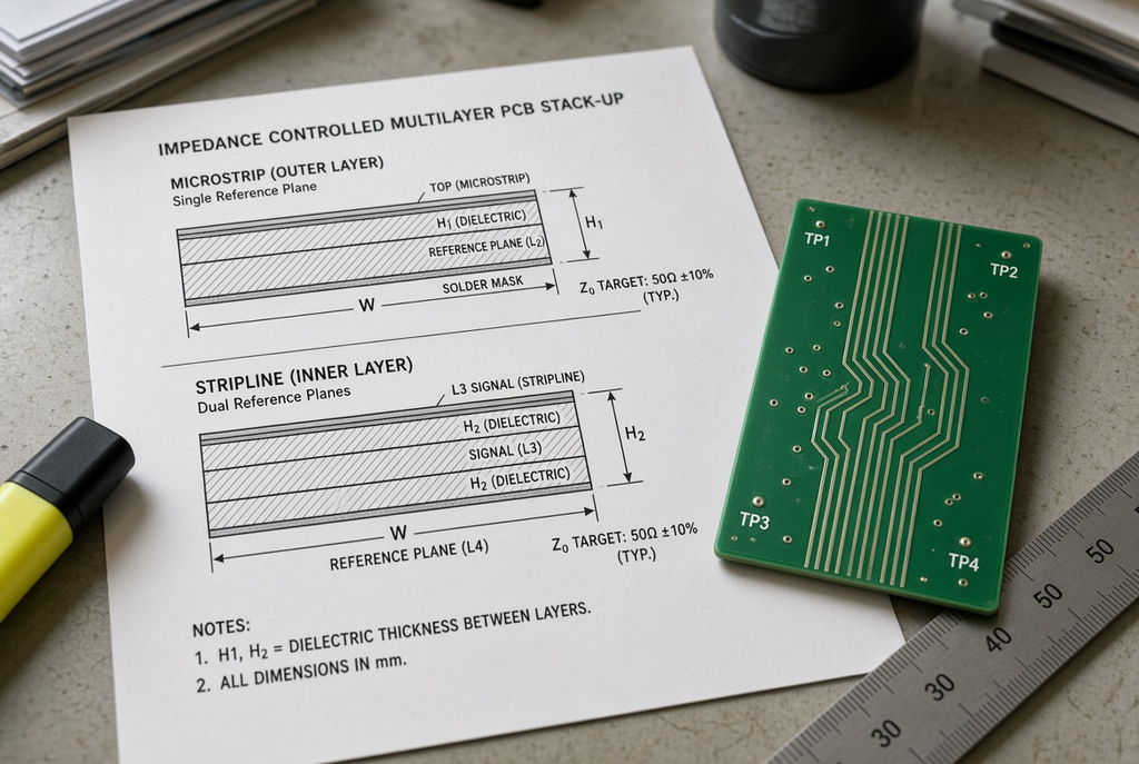
A PCB impedance stack-up is used to provide a repeatable geometry: a known dielectric, a solid reference, and a trace width the shop can etch, to get controlled-impedance nets. If these three pieces are inconsistent across layers or inconsistent across boards, then drawing a target for the impedance is just a dream.
Reference Planes, Trace Geometry, and Dielectric Thickness
The trace width, spacing, thickness of the dielectrics, dielectric constant of the PCB and a continuous reference plane are the factors that controlled impedance PCB design relies upon. Microstrip on outer layer – one reference under the trace, one upper solder mask. Stripline’s planes are found on both sides. If the reference is split or if the dielectric thickness changes along the way, or if the number of net hops is different in the target layer but there is no transition design, either structure fails.
Avoid placing impedance controlled nets on layers with no documented reference, and on layers that the fabricator cannot model. Changing layers mid-net is permitted when the design considers the via, the reference change and the new geometry. Coupons change layers in cases where there is no space in the channel, but there is no plan of returning to the previous channel, and the product rings.
Working With the Fabricator on Impedance Modeling
Communicate impedance requirements as early as possible; single-ended and differential targets, which layers are involved, any length-match or loss notes. Then have the fabricator model the stack against what the actual cores, prepregs, resin contents and process windows are used in the process. They have a model with foil type, etch-back and a dielectric tolerance which a typical field-solver default does not have.
Use the first stack drawing as a proposal. The useful loop is: say that you want to do something electrical, the fabricator suggests a construction that’s able to meet impedance and thickness specs using qualified materials, you check return paths and copper balance, and you then freeze the stack before you finish the layout. The cost of late stack changes after routing is high. The focus of the review is early stack changes.
Common Pitfalls in PCB Stack-Up Design
Most failures due to stack-up are not unusual. These are blamed on premature locking of construction, but also due to a lack of mechanics or the use of materials which cannot be reproduced in the shop.
Designing the Stack Without SI/PI or Fabricator Input
The most common error is during schematic review with no SI/PI or fabrication input – locking the layer count and total thickness. The drawing seems to be complete. After this, it is found that the “high-speed” layer does not have the adjacent ground, two rail sharing a chopped plane or the dielectric which the CAD default assumed is not a stock core. Symptoms can range from missing impedance coupons to any noise when powered on or a stack change at the last moment after parts have been installed.
Take the impedance list, power-domain map and a preliminary layer assignment to the fabricator before committing to routing. Cost of a single page stack will be less than a respin.
Unbalanced Stacks and Warpage After Lamination
Bowed boards are caused by the asymmetric layer order and Cu coating. Both the press cycle and the reflow profile will heat and cool the laminate. The first side of the stack is solid, heavy plane and the second side is sparse signal copper, the board is a set. Pick and place fights against warped panels, connectors or BGAs with uneven seating.
Assess the coverage of copper, layer by layer, and not just the total thickness. If the coverage is skewed (asymmetric) state the name of the problem and ask the balancing procedure to be performed without disturbing the electrical reference.
Over-Constraining the Stack With Non-Standard Materials or Thicknesses
Exotic laminates, unusual thicknesses of dielectrics and combined copper weights are not a standard construction for the fabricator, which increases cost, lead time, and repeatability concerns. The first lot could be a success. The second lot can be of another prepreg lot or be a different optional core and can be both out of impedance and out of thickness.
Start from the fabricator’s qualified material sets, which include material sets and core/prepreg options. Request a special construction, if these options do not meet the needs of the electrical or thermal requirement. Don’t copy and paste the requirement and tolerance from a different project; specify the requirement as a target and a tolerance.
Practical Stack-Up Planning Workflow
The short loop to remember the planning steps is to: Record electrical and mechanical requirements/constraints; Specify roles for each layer; Identify the material class; Model the impedance with the fabricator; Then freeze construction prior to layout.
Start From Electrical Requirements and Board Constraints
Write the following constraints first. Estimate number of layers depending on the density of routing and number of high speed nets. Note down the Impediment Objectives and the layers to be included in the Impediment Objectives. Graph power domains and pours that need planes. Note mechanical/thermal limits on housing, note board outline, and finished thickness limits from connectors/encasing.
The stack is a result of that list. Return paths and impedances are broken when it is assumed that “we always use eight layers, 1.6 mm” and the electrics are shoved into this box.
Iterate With the Fabricator on Materials and Construction
Provide the draft stack, impedance table, copper weights and thickness target. Query the fabricator for one that is proposed by them that fits those numbers based on core/prepreg build and materials they qualify. Review the concept of adjacency of planes, copper balance and if there would be an advantage in switching layers for impedance and warpage.
Think of the stack-up as a design artifact to which all people are part. The current map and net classes are property of the hardware. SI/PI has the ownership rules of the impedance and reference rules. What’s pressable, etchable and repeatable is manufacturing. The stack of frosted fish ought to be an item that all three can sign
Treat Stack-Up as a Cross-Disciplinary Design Artifact
PCB stack up design is a combination of signal integrity, power integrity, thermal characteristics and manufacturability. Single input is the number of layers. The factors that will make or break whether the board can meet its electrical requirements and whether it can be duplicated are the selection of the reference plane, thickness of the dielectrics, weight of the copper, copper balance and copper material class.
Engage SI/PI, hardware, mechanical and manufacturing stakeholders prior to high-density layout. Describe clearly and comprehensively the impedance and power requirements. Work on a construction with the fabricator which they can model and repeat. Better than a pretty on a slide production-ready stack is an electrically honest stack that can be used for production.