No PCB trace width vs current is a number to be copied from one board to another. The width is a thermal and fabrication choice such as copper weight, inner versus outer layer, allowable temperature rise and how the trace will etch all influence this amount of current that can flow through the copper without causing it to run hot or drop in voltage. If you’re making a 20 °C budget and a 10 °C rise, or a plated outer rail, or inner rail buried, that will not be captured in the calculator and is not a nominal 1 oz foil.
The common pitfall is that the calculator is considered to be the standard width. These tools are based on simplified models and nominal copper. Real boards include the following: limits of plating, limits of etch undercut, adjacent planes, and limits of stack-up. Those don’t show up on the drawing, traces overheat, rails drop more voltage than the circuit can afford, and/or impedance models change with time, or the board ends up paying for copper it didn’t need.
What PCB Trace Width vs Current Actually Depends On
The industry current-capacity models assume that a trace is a copper cross-section that is heated by the current. That’s just the width of that cross-section. The final thickness after plating and etch, the position of the layers, the weight of the copper and the temperature increase that you are willing to accept all affect the result. All those same choices impact stack-up thickness, controlled impedance, and the amount of etch space provided adjacent to the rail.
Copper Weight, Layer Position, and Finished Thickness
The nominal foil is the foil that is applied to the laminate which is typically described in ounces of copper. The position of layers is not as complicated as it sounds, as it is either inner or outer. The copper seen by the current is the finished thickness after plating and etching.
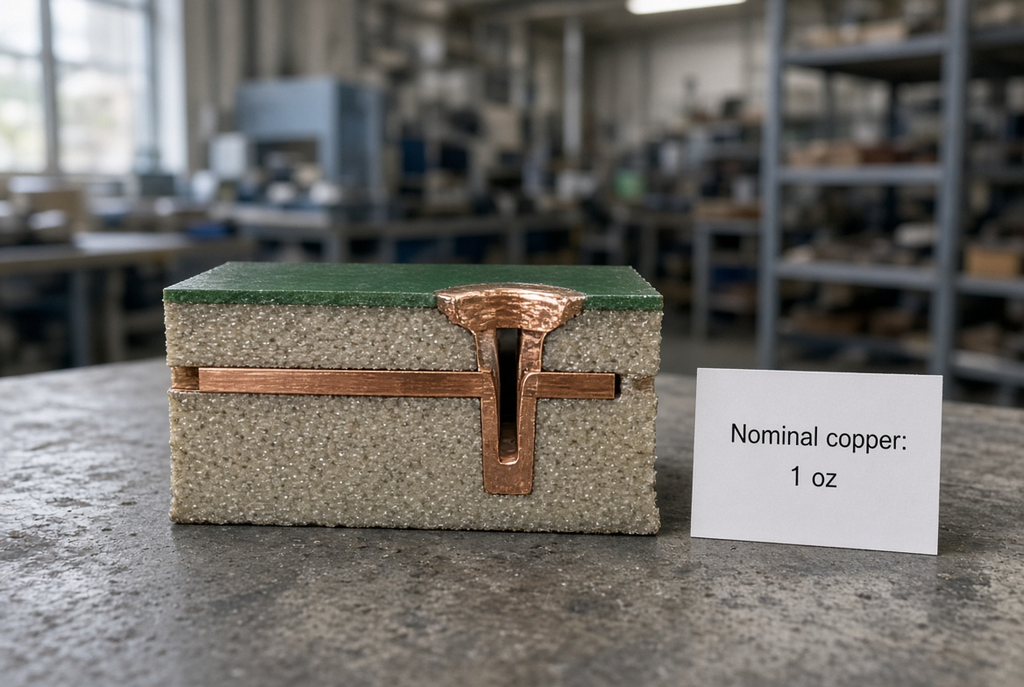
The problem is putting in 1 oz nominal into the calculator and then expecting to get the same amount of current capacity on each layer. Inner copper is typically foil, patterned and then embedded in the stack-up. Often, the outer copper will be thinner than what it is finally finished as, or it will be plated up, so a note of 1 oz finished could be 0.5 oz copper foil. The same weight, but different finished metal, different heating.
Allowable Temperature Rise and Ambient Conditions
A 5 A rail may be designed to be the same size on a copper of the same weight and still give different widths to two designers. One can be used for a temperature increase of 10 °C over ambient. The other allows 20 °C. The first design requires more cross-section of copper. It also has lower voltage drop for extended runs. The second design is hotter for the same current and could be OK in an open air and not in a closed box.
But the assumption of temperature rise in PCB traces is not the default. Record the rise you used, and the ambient you assumed, in the design notes. A calculator which does not display those two numbers is not providing a unique answer. It’s providing you with one point on a curve.
Trace Width, Current, and Temperature Rise: The Practical Relationship
The IPC documents give models and curves to show the relationship between width, copper thickness and temperature rise. Those models are handy. They are not the only “right” width for a particular “A” rating and they are not an alternative to making the actual width checks for the stack-up you will be assembling. The numbers which follow are approximate. Verify them with the completed copper, layer location, and etchability of the board, DO NOT verify with a screen shot of the previous project.
Temperature Rise, Not Just Current, Sets Trace Width
Current sets how much heat the copper must shed. Allowable temperature rise sets how much temperature you will give that heat. Width and copper thickness are the levers you still control after those two inputs are fixed.
| Current (guideline scene) | Temperature rise assumption | What changes the width |
| Same continuous current on a short outer rail | 10 °C above ambient | Tighter rise budget needs more copper cross-section—usually a wider trace, heavier copper, or both |
| Same continuous current on that rail | 20 °C above ambient | A larger thermal budget often allows a narrower trace at the same copper weight |
| Same continuous current moved to an inner layer | Same 10 °C target | Inner copper usually needs more width than an outer trace at the same nominal weight because heat leaves the board less easily |
The longer the power rail, the more voltage drop, which further increases the temperature. Even a wide cool trace will not feed a load if the run is long and the copper is thin. Measure across and across up first, and then measure the ohmic drop with the actual length.
Inner Layers and Outer Layers Do Not Carry Current the Same Way
The inner layer traces are started as foil on the core. This foil is cleaned, etched, and encased within the lamination. The outer layer traces are generally first on a thinner foil and then plated with copper prior to final etching. The 1 oz is a process history that is different from 1 oz finished.
The difference is hidden in a layout with the same width of the inner and outer traces for the same current. The outer conductor can be thicker following plating. It also dissipates heat off of the board surface. The inner conductor is placed between the dielectrics and relies on the stack-up to remove heat from the inner conductor. For the current when real and continuous (motor drivers, LED drivers, DC-DC outputs, high current digital planes), consider the inner and outer currents separately.
How to Choose Trace Width for Your Board
Walk the decision as the fabricator will need to construct it: continuous current and temp rise allowed, voltage drop on long rails, passing heat to nearby copper, impedance and loss on the same layer, etc., then etch and cost. Neither a broader trace nor heavier copper nor a real thermal path can replace a plane.
When Standard Widths Are Enough for Digital and Mixed-Signal Boards
Power-rail widths are not required for most of the digital or mixed signal nets. Fine etch, impedance control, more important than ampacity. A common approach in that environment is to use 0.5 oz or 0.5 oz on inner signal layers, since the etch can closer the gap in the spaces and the impedance model remains closer to the stack-up note.
The problem is that if outer layers are using it, copying the width onto inner signal layers just for that reason. The inner foil, plating and heat flow are not the same. Maintain signal geometry on stack up. Power geometry for the present and the increase tone.
When Wider Traces or Heavier Copper Are Justified for Power
Where current is flowing, where the rail is long enough to effect voltage drop, or where the copper is itself a part of the heat path, PCB trace width is justified for power design (power stages, LED drivers, motor bridges, and all dense DC-DC designs). Copper is a material that conducts heat laterally. The heavier copper makes up the cross section but does not use as much routing space.
A wide trace is NOT a “heavy-copper power board. Everyday foil, 2 oz and above foil have different etch times, minimum space requirements, registration stresses, and soldermask behavior. When the cross section is the focus of the design, request heavier copper. Don’t request it as a universal upgrade on a board that had just a wider 1 oz rail.
What Gets Harder as the Trace Width and Copper Increase
Traces tend to become less comfortable when space is less, soldermask dams are placed and when the copper is increased.The more the space is reduced, soldermask dams added and copper increased, the less comfortable the minimum space becomes.
How to Specify Trace Width and Current So Fabrication Does Not Guess
No treatment applied to the copper and no copper pieces with the finished target.No treated copper and no finished target copper pieces.
Callout Matrix for Trace Width and Current Fabrication Data
| Write this in the fabrication data | Do not leave it implied |
| Inner-layer foil weight, layer by layer if the weights differ | “1 oz everywhere” when inners and outers are not the same |
| Outer-layer finished copper, or starting foil plus the finished target | Calculator copper that ignores plating on the outer layers |
| Units when thickness is given in μm or mil | Mixing oz on one layer and mil on another with no conversion note |
| Copper used in the impedance model, if impedance is controlled | An impedance stack-up that assumes different copper than the power note |
| IPC class only if the class is required | “Standard copper” with no class and no finished target |
| Copper-to-edge, heavy-pour, or isolation notes that change etch | Fine pitch next to a heavy pour with no keep-out language |
Where the Trace Width and Current Note Should Live
Place note on stack up and fabrication drawing. That will be the package that CAM will use. The common way to make the wrong board is to use a Gerber set that doesn’t contain a copper note, a stack-up PDF that doesn’t have 1 oz information, and a quote form that doesn’t contain 2 oz information. Take 1 controlled note. Adjust the drawing if the assumption for the rise changes or the copper changes. Don’t include the correction in an email message.
Cost and Yield Effects of Trace Width and Current That Do Not Show Up in the Calculator
The heavier the copper, the more expensive the foil and etch. It also increases the likelihood of a fine space next to a power pour not releasing. This is the other side of the trade, with a real cost: a 1 oz rail that’s never sufficient can send a board spinning, and a spin isn’t cheap.
It is important to compare quotes after you have started and finished copper, layer weights and minimum space are equal. A lower cost line item with a lighter finished copper is NOT the same board. These are not just layout editor features, but also trace width and copper weight.
Frequently Asked Questions
Is trace width the only factor that sets current capacity?
No.: Width is one side of the copper cross-section. The amount of current the trace can carry depends on the copper weight, the thickness of the copper after the plating and etch, the inner versus outer layer, the allowable temperature rise, ambient conditions, and the surrounding copper.
What is the difference between trace width and copper weight for current?
The lateral size of the conductor is width. The nominal foil is the copper, the finished thickness is after plating and etch. Cross-section is heated in the current heat. To update a width only, or a weight only is an incomplete request.
Should every layer use the same trace width for the same current?
No. It will not be the same on the inside (inner foil) and outside (outer plated copper).No, it’s not the same on the inside as the outside (inner foil and outer plated copper). When the current is continuous, the size of inner and outer rails should be done separately.
Does a wider trace always carry more current?
A wider trace results in lower resistance and typically will run cooler at the same trace thickness, with a higher current carrying capacity at a given temperature change. It will not cure a plane, heavier copper or a thermal path, and a short wide stub will not cure voltage drop on a long thin rail.
How should trace width and current be written on a fabrication drawing?
Name the layer, and specify the starting foil or finished copper, plus the units used, and if there are different layers inside and out. If the impedance is controlled, then say the type of copper used in that model. If necessary, give the name of IPC class. Not just in the quote form, but keep that note on the stack-up and the fabrication drawing.
When is a heavier copper PCB the right question, rather than a wider trace?
Request heavier copper where the design requirement is the cross-section and not the thickness of the copper itself (i.e. heat spreading within the copper or tight routing space or a requirement for continuous high current). Request a wider trace if sufficient for the layout, everyday foil will do. Heavier copper, it is a construction decision, and not a wider line on the same stack-up, that alters the etch, space, and soldermask.