
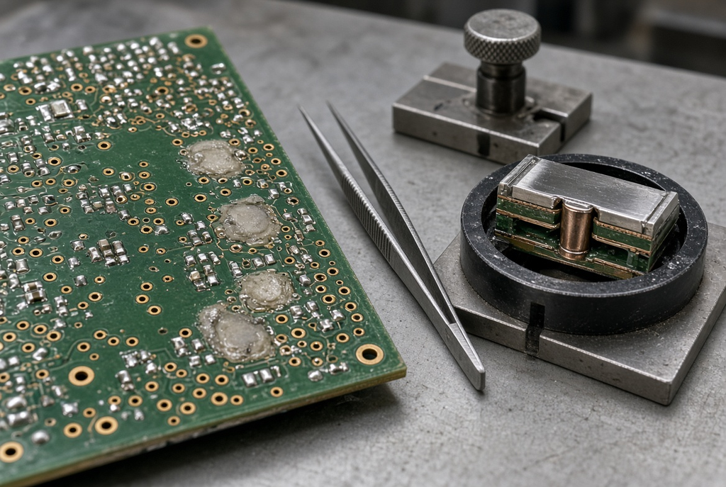
PCB Delamination: Causes, Detection Methods, and Prevention
Hardware engineers, PCB designers, and quality or NPI teams often treat delamination as a single-cause factory defect. This guide separates that habit from the real problem: interacting risks in stack-up, materials, moisture, lamination, reflow, and rework. Use it to judge new designs, investigate field or production failures, and decide which design, storage, and process controls actually reduce risk.
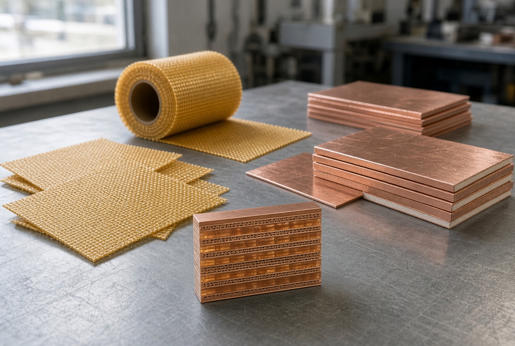
What Is PCB Prepreg? Materials, Properties, and Lamination Functions
Hardware engineers, PCB designers, and stack-up engineers often treat prepreg as glue. This guide explains what PCB prepreg is, how resin content and flow set dielectric thickness after lamination, and which stack-up choices actually hold impedance and keep warpage under control. Use it when planning dielectrics, ply count, and lamination strategy on multilayer boards.
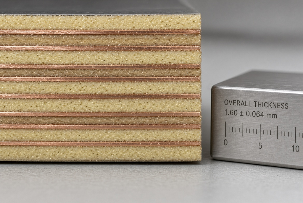
PCB Core vs Prepreg: Key Differences in Multilayer Stack-Ups
Hardware engineers, PCB designers, and SI/PI teams often treat core and prepreg as the same dielectric. They are not. This guide explains each role in a multilayer stack-up, how thickness control and symmetry affect impedance and warpage, and how to plan a buildable core/prepreg construction with the fabricator.
Copper-Clad Laminates: Structure, Types, and Role in PCB Manufacturing
This guide is for hardware engineers, PCB designers, and sourcing teams who treat copper-clad laminate as a black box. It explains CCL structure—foil, resin, and reinforcement—then maps common types to etching, impedance, thermal behavior, and reliability so you can discuss materials with a fabricator instead of locking a part number too early.
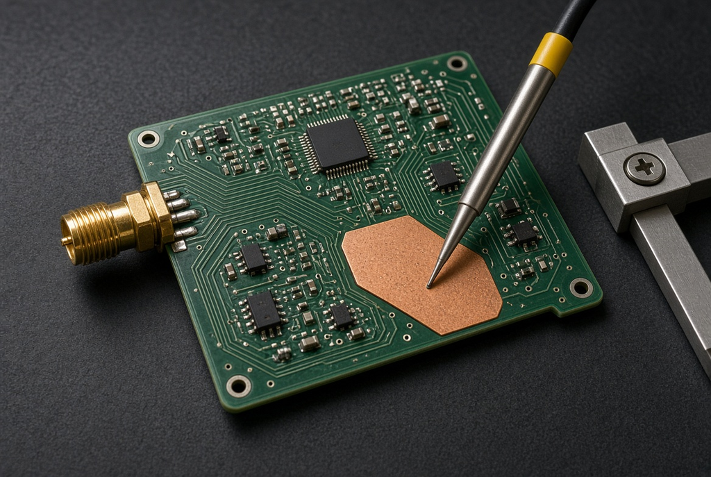
PCB Substrate Materials: How to Choose for Electrical, Thermal, and Mechanical Performance
This guide is for hardware engineers, PCB designers, and sourcing teams evaluating PCB substrates before they lock a stack-up or request a quote. It replaces brand-name or habit-based picks with a three-axis check of electrical, thermal, and mechanical performance, then walks through a scoring workflow and the pitfalls that trigger late material changes.
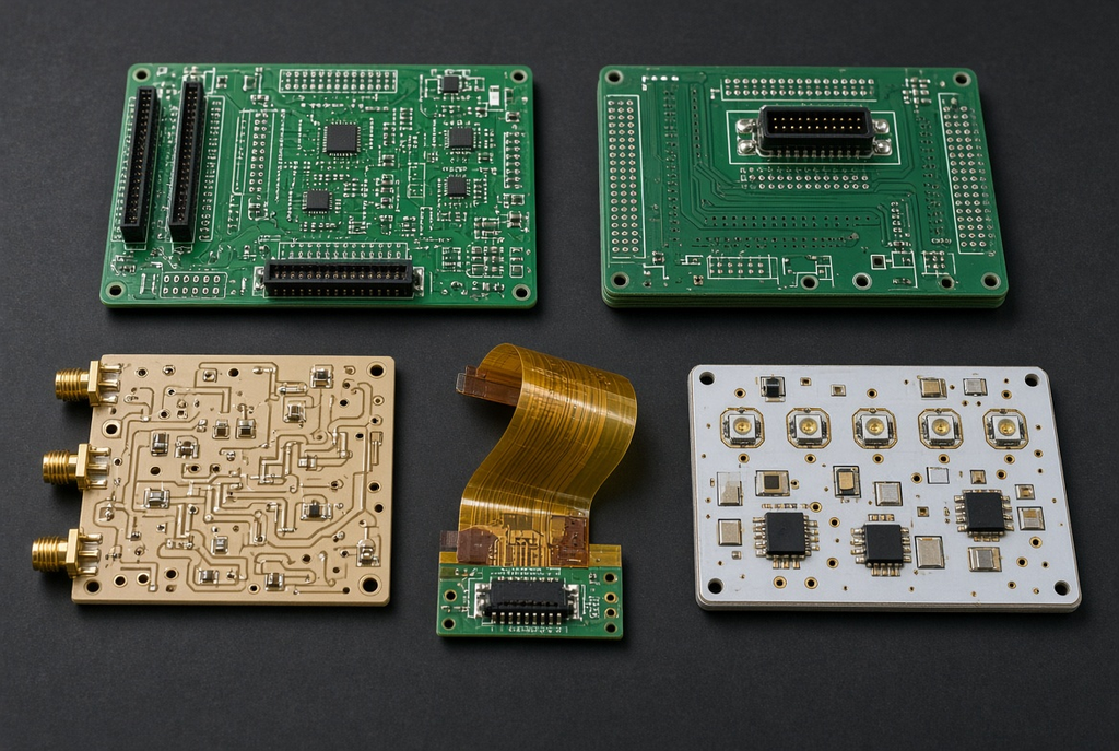
PCB Laminate Materials: FR-4, High-Tg, RF, Flex, and Metal-Core Options
Hardware engineers, PCB designers, and sourcing teams often treat every board as FR-4. This guide separates standard FR-4, high-Tg, RF, flex, and metal-core laminate families by application risk, then walks through the decisions to make before locking a stack-up or requesting a quote.
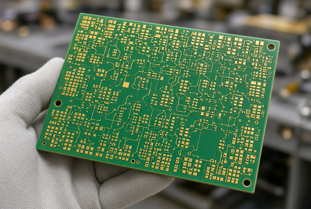
PCB Materials Explained: Substrates, Copper, Solder Mask, and Surface Finishes
Hardware engineers, PCB designers, and purchasing teams often treat “FR-4, 1 oz, green, ENIG” as a complete bare-board spec. It is not. This guide separates substrate, copper, solder mask, and surface finish into the four callouts a fabricator needs, and shows what to put in the notes before you request a quote.
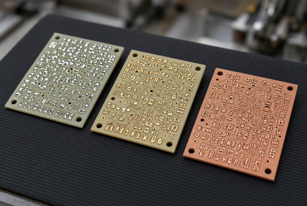
PCB Surface Finish Types: A Complete Comparison for PCB Design and Assembly
This guide is for PCB designers, NPI engineers, and hardware teams choosing among PCB surface finish types before they release fabrication and assembly data. It compares HASL, ENIG, OSP, and immersion finishes, then maps pitch, reflow, shelf life, and contact wear so teams can pick a PCB finish for assembly instead of defaulting to habit or price.