A team locking a 1.6mm FR-4 board is pretty common, because that’s the board that was used for the previous project. The default option for the thickness of a PCB is not checked. It is a mechanical and electrical decision, meaning that it is an engagement of a connector, an enclosure clearance, a connector stiffness and warpage, a dielectric spacing for impedance, and how a panel will behave when it is assembled. If one chooses a value early, before drawings and stack-up are determined, then there is no change of value late and boards that are hard to repeat on the next order.
A myth exists in the minds of some fabricators that it is always possible to supply 1.6 mm FR-4 without any consequences. The thickness commonly employed; finished thickness will vary according to core and prepreg build, copper weight and number of layers. Even though uncharacteristic values may be constructed, they are more frequently not a part of a store’s regular designs. Application should push the number and the fabricator should check the construction so that he can tag it again.
Common Standard PCB Thickness Values and Where They Are Used
When engineers refer to board thickness, they’re typically referring to finished thickness, once the material has been laminated, plated, had solder mask applied and surface finish. A short list of nominal values is the ‘standard’ fabrications. These are industry averages and not a guarantee that the cores will be located in all shops nor a guarantee that the same tolerance would be achieved on each construction.
Typical Thickness Values in Everyday Designs
Generally, the thickness of rigid FR-4 materials that can be found is 0.8mm, 1.0mm, 1.2mm, 1.5mm, 1.6mm and 2.0mm. When there is a need for stiffness or current handling, thicker constructions show up. On the thickness side, the 0.062 inch thickness of the card itself was the norm for many edge connectors and card guides, and is therefore the typical thickness of the commercial boards.
Avoid slicing on the target number, slice using a tolerance on the number on the fabrication drawing. Placing copper weight, putting the plating in holes, thickness of the mask and type of core/plating combination all effects finished thickness. Board #1 and #2 can be made of different stacks and be both tested as “1.6 mm”. Availability is also according to the normal material set of the fabricator. The same value used in one location or store can be a special build in another location or store. Availability is also based on the fabricator’s regular material offerings. A value that’s available in one part of the country or store might be a special build in another.
Application Examples for Different Thickness Ranges
Thicknesses tend to come in bunches, according to product constraints, not fashion.
For small component products, for low-standing parts and for assemblies that are stacked, thinner boards (0.8 – 1.0 mm) are clearly visible in every 10th of a millimetre that has to be fought in a housing. They are used for storing height and weight. There’s also some give, which means that you need to take a second look at large outlines, heavy connectors, or unsupported spans.
The 1.2–1.6 mm version is used for most general purpose industrial controls, communications equipment and consumer electronics which reside in a standard enclosure. The connector family, card stand-off and the card slot are all optimized for 1.6 mm board thickness, and so is a 1.6 mm board.
The boards are available in 2.0 mm or larger sizes for larger outlines, mechanical load or when heavier copper is carrying current. Extra thickness can sometimes be bought as stiffness and to give thermal mass. It also can withstand enclosure, connector opening and assembly fixture pull for a thinner card.
These are only patterns, not rules. If the I/O connector requires it, a small industrial board can be 2.0 mm thick. The product must close at a certain height, a large consumer board can be 1.0 mm. You can’t begin with the final Gerber that you have reused.
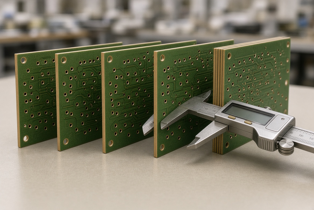
Mechanical Design Considerations for PCB Thickness
Design review time is spent the most with Electrical stack-up. The thickness problems can first appear, though, as a mechanical problem like a card that is not seated, a house that will not open or a panel that is oil-canned on the SMT line.
Connector Compatibility and Edge Fit
There are too many edge connectors, card-edge sockets and board-to-board connectors that are one board thickness and have a narrow tolerance on that thickness. It’s not a “so-so” preference when it comes to PCB thickness and compatibility of connectors. Often when the board is thin, it’s not conducive to the contact system, leading to poor wiping or loss of normal force on the contacts. A thick board can cause the card not to fit in the slot and/or spread the housing and create stress on the solder joints on the mate.
Before the thickness note is frozen on the fabrication print read the connector datasheet and mechanical drawing. Confirm the thickness of the board, any tolerances, chamfer &/or bevel angles and/or any keep-out distances for contacts near the edge of the board in card-edge designs. The pressfit hardware, card guides and backplane slots are not an exception. When you have to change thickness after buying, it is a costly process to discover that two numbers don’t match when you purchase the connector.
Stiffness, Warpage, and Enclosure Fit
Among the most powerful levers affecting bending stiffness is the thickness. The thinner the board, the more it will flex when inserting the connectors, under the pressure of the screw clamps, on vibration and handling. The flex can bend or break large packages, cause connectors to pop up or cause the keypad or display to rise off the front panel.
The thicker the board, the more warped the PCB will be. Thin, large or Cu-inbalanced boards are more susceptible to bowing due to reflow and to remain bowed after cooling. It will be more resistant to that movement, but will not cure an unbalanced stack that is way out of whack. The excessive thickness yields the reverse effect – the board will not drop into the boss shape, the cover will end up on one corner rather than on the gasket, or mounting screws will pull the cover into a dish and load the components.
The enclosure fit, which is composed of small small parameters, finished board thickness, mask/finish buildup, component height, standoff length, cover crush. The mechanical model determines the fabricator’s intended thickness of 1.6 mm, as well as whether the fabricator used a thicker version as a “legal thickness”, which means that the cover may not close. Lock the thickness as you locked the outline.
Electrical and Stack-Up Implications of Board Thickness
Finished thickness is not an additional spec that you select once you have selected the layer count. Total is the total of the stack.
Layer Count, Core/Prepreg Build, and Overall Thickness
The thickness and stacking of multi-layer PCBs is a problem from two angles. All cores are aggregated, plus prepreg sheets, copper foil and plated copper. The more layers (or thicker copper), the larger the board will be, unless the dielectric stack is made thinner.
Such compensation is capped. Very thin dielectrics can be harder to control, have higher resin content sensitivities and possibly be less tolerant of glass-weave effects when compared to other thicker dielectrics. In a very high build, extra prepregs may need to be used which are not commonly found in the fabricator’s library. The drawing must read “8 layers, 1.6 mm, 2 oz outer,” which means that the stack must be achievable with actual cores, and not just a spreadsheet sum.
Impedance Control and Dielectric Thickness
The distance that the trace is above the reference plane or “dielectric height” is also a factor in controlled-impedance traces, as is the width of the trace and the weight of the copper. The overall thickness of the board is not the impedance itself, but rather it dictates mechanical target setting and the resulting available dielectric heights.
Too thin of a board may not allow enough space between the plane and the signal the impedance model requires. If it’s quite thick, more plies can be placed above or below the impedance pair, or the impedance pair can be inserted into the core that the fabricator doesn’t want to use. In either instance, a width change, different glass style or a non-standard build of the construction may be required.
Avoid breaking up the word “impedance” and “thickness”. Avoid putting the housing in the freezer at 1.0 mm and finding out the 90 ohm pair requires the rest of the stack to contain a dielectric which this cannot supply.
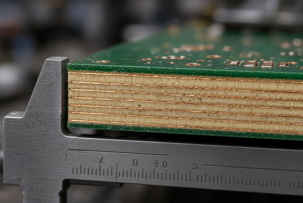
Common Pitfalls When Specifying PCB Thickness
The majority of thickness issues are not uncommon. They are the product of a default number, a special number that no one has checked or a change performed after the remainder of the product has been drawn.
Using 1.6 mm as a Universal Default
All the stack-up, all the impedance model, all of the connector 3D, all the enclosure, all of the stand-off drawing and in some cases, all the test fixture are locked documents.The stack-up is one of the few documents that are locked, with the impedance model, 3D connector, enclosure, standoff drawing and sometimes the test fixture. After they are released, it’s not a one line change on the fabrication note.
The stack must be put back together again. The width of the impedance traces may need to be changed. Mechanical clearance is capable of disappearing. No longer can connectors locate and line up with card-edge bevels. The PCB team found an even more economical core for the plastic housing and the tooling doesn’t move. Determine thickness while mechanical and electrical owners are still free to select their models together.
Ignoring Fabrication Realities for Non-Standard Thicknesses
If you don’t use one of the listed values, such as 1.7 mm, 2.3 mm, then it can be valid for mechanical reasons. It will also require a non-standard core/prepreg combination, a higher level of process care and a more difficult repeatable construction on the second and third order.
That’s construction, not the millimeter figure, that has cost and schedule effects. For a shop that is building 1.6 mm and 2.0 mm all day, they can still require a special 1.7 mm press book. If the odd number is not due to an “odd thickness” CAD dimension that was not rounded to a common FR-4 thickness, then you are purchasing complexity for no product benefit. Indicate early if the odd number is needed and ask what standard builds lie between the odd number.
Changing Thickness Late in the Design Cycle
The stack-up, the impedance model, the connector 3D, the enclosure, the standoff drawing, and in some cases, the test fixture are all locked documents.The stack-up is one of several locked documents, along with the impedance model, the connector 3D, the enclosure, the standoff drawing, and sometimes the test fixture. Once they are released it is not a one line change on the fabrication note.
The stack needs to be reassembled. New widths for impedance traces may be required. Mechanical clearance is capable of disappearing. Connector openings and card-edge bevels can no longer line up. The PCB team found an even more economical core for the plastic housing and the tooling doesn’t move. Determine thickness while mechanical and electrical owners are still free to select their models together.
Practical Guidance for Choosing and Specifying PCB Thickness
The selection of PCB board thickness is a series, not a guess. Mechanical constraints first, then a stack that can run the number that the construction fabricator already knows.
Start From Mechanical and Connector Requirements
Prior to selection of a favorite dielectric, the connector datasheets, the enclosure section views, the standoff stack and any vibration/flex requirement must be pulled. From those inputs calculate the desired finished thickness, and the desired tolerance level that the product can accept.
Now take this target and go to the electrical stack up. Try to work out the conflict while the housing is a model, don’t try to cut steel to clear an impedance pair. Thickness of PCB design considerations start from mechanical drawing first and then advance to the layer stack.
Align Thickness With Standard Fabricator Builds Where Possible
A thickness similar to that of a typical fiber matrix and prepreg assembly of a fabricator is more easily quoted, more easily held and more easily purchased again. Discuss thickness, copper weights, number of layers and comments on impedance at an early stage. Accept a standard construction (which is recommended by fabricator) that meets the mechanical number and electrical requirements.
If the product actually needs a nonstandard thickness, be aware of the reasons, and be willing to consider a lesser-known construction. Please, never embed an odd thickness (other than “as per Gerber”) in a note. If the stack is to be designed to a thickness or tolerance or a limit based on a connector, then specify the finished thickness, tolerance, and note that it is a connector-driven limit.

Summary Guidance – Treat PCB Thickness as a Cross-Functional Requirement
A common requirement is thickness of boards. It impacts on connector engagement, enclosure clearance, stiffness, warpage, stack-up and impedance spacing. Mechanical, electrical, and manufacturing owners need to see the same target prior to the outline.
Examine the connector and box initially. If possible, choose a standard thickness of FR-4. If it is not something that is readily available, make sure to explain clearly and precisely what thickness and tolerance is needed and make sure that the construction for the next order can be similar. The early design parameter chosen is the thickness. Thickness selection is a late decision, re-design.