Many boards are set up to have the laminate as a mechanical carrier only. In fact, the actual thermal resistance of the PCB is the resistance that occurs between the junction to ambient path through the substrate, copper and via. That resistance is not a universal characteristic of “FR-4.” This is a design variable which includes dielectric conductivity, plane layout, copper weight and via arrays, all of which will determine heat removal from a pad and any hotspot conditions, first article.
It is not as easy as simply adding copper, because it will not help to solve the problem. If there is no connected path in to planes, a thermal via, metal core or a heatsink, there is no problem to use the foil as a warm island in the plane. The subsequent sections of this document describe those levers, beginning with the one that a power-electronics or NPI team should consider first.
Understanding PCB Thermal Resistance as a System
No “dump heat into the board” event is there in a MOSFET, LED array or motor-drive stage. Heat flows from the die to the package/solder joint, and then to copper and dielectric and to the air, and/or to a heatsink attached to the chassis. The fan can be placed on the opposite side of the case to the package to allow the case temperature measurement without any temperature bottleneck taken at the board level as is the case in a closed configuration.
Do not think of using the PCB as a substitute for the rest of the chain.
From Junction to Ambient: Where the PCB Fits
The path can be thought as: junction → case (or exposed pad) → solder and copper pad → board structure → surface or hardware which dissipates the heat to the environment. The heat transfer in that middle length of PCB is conduction, in the first two ways, and in the third, much slower, through the dielectric. Convection and radiation start only when heat reaches the surface to which they can exchange heat with air or metal enclosure.
It’s necessary in the power electronics arena. A device with a large thermal pad in need of putting heat onto a small area. In the case of a thin copper island on top of standard laminate, only the first few millimetres of the path will make the difference to the temperature rise. The board is indeed doing work in the form of heat. It is inadequate for use as a heatsink by itself, and it will not remove a package if the package was not provided with a rejection path.
Don’t remove published θJA or θJC values. Those numbers are a package that is tested and defined under a certain condition. Do not use for your stack-up, your plane cuts or your via field. The board level resistance will need to be estimated based on the construction that you send to the fabricator.
Series and Parallel Thermal Paths in a Board
Heat is a non-discrimination rider. It will split on any conductor on which it can find itself, namely:
- When the pours and planes are wide, a lateral spreading will develop in copper.
- Thermal Vias for vertical conduction
- Thickness of the dielectric that exhibits slow conduction.
- Conduction to attached metal core, heat spreader or chassis boss.
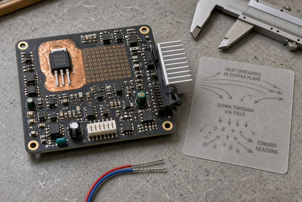
The paths are parallel to each other. For the lowest resistance path, much of the heat is carried and making a better path on this path will not be of much benefit if there is a “neck” in series with the package pad. A four ounce pour that leads to a dead-end is a parallel path. Pad under dense via array and cut up ground pour is a vertical path with no ability to move.
The rule of thumb is to tackle the most important constraint first. The FR-4 designs that are often the limiting factor are through-thickness dielectrics. The problem could be either the narrow dielectric between the circuit foil and metal plate or the connection between the metal plate and the housing. It is only if they are limiting the design that copper weight (by count) and the selection of materials can help the design.
How Substrate Materials Affect Thermal Resistance
Copper is a good conductor of electricity. Not the container (resin/glass) that the copper is placed in. From there on, it is a problem of the quantity of heat that must flow through the thickness of the board and not a cataloging exercise of choosing materials.
Dielectric Thermal Conductivity and Board-Level Heat Flow
A hot pad built using the dielectric thermal conductivity type of PCB construction is local. The heat that is not conducted through the copper or a plated hole must pass through the resin and the glass, which are many orders of magnitude less conductive than copper. For this reason, it would be beneficial to have a wider top-layer pour to adjacent components and a steep gradient through the stack, if there is no vertical pour.
Two consequences follow.
Firstly, spreading in the plane is different than spreading through the plane. Planes and heavy copper are good for the first job. Avoid doing the second in itself. Secondly, you are no longer “tuning FR-4.” You’re wondering if the dielectrics are a good thermal resistor to be in series with the package.
The non-value sensitive glass-epoxy products drive the selection of conductive special laminates, insulated metal substrates and metal cores. They don’t take copper geometry away. These are inversions – they are switching which part of the stack is the limiting factor.
When to Consider High-Thermal or Metal-Core Substrates
If your typical industrial control, comms and limited-power conversion applications can be satisfied with the standard FR-4, disciplined copper and disciplined vias will suffice. When dissipation is targeted, it’s different with high-powered LED arrays, small-sized motor drivers, RF power amplifiers and even power modules that fit into a small volume within a closed box.
In such cases, the thermal resistance of metal-core PCB is helpful as the metal plate will offer a low resistance path under the circuit layer, ensuring the circuit is constantly heated. It is not “zero resistance” because the heat has to pass through the thin dielectric between the foil and the plate. It is a series stack consisting solder/copper/thin dielectric/metal plate/chassis/air.
That heaped-up pile has some trade-offs. Signal layer density, control impedance and the ability to stack multiple layers of signals on a metal-core or single-layer insulated-metal board are more challenging than those of a traditional multi-layer FR-4 stack-up. Cost and rules for fabrication change. The mechanical stiffness and CTE behavior alters. All of these can’t be used as excuses not to build when the thermal budget requires it. There are reasons for its own, however, to choose it intentionally and what considerations the fabricator may need to take into account before the stack-up is solidified.
Copper Weight, Planes, and Trace Layout as Thermal Levers
When the dielectric is setting the through-board limit, the copper is setting how far the heat will travel before it must traverse the dielectric’s through board limit. Not only is the copper weight related to the area and thickness of the PCB, but also most significantly must be connected by its connectivity.
Using Planes and Heavy Copper to Spread Heat
A thermal pad may be fixed to a solid plane, and may spread a solid plane. The heat generated inside the small pad area is conducted laterally across the foil, and then it has a larger pad area to conduct heat into either vias or the opposite side of the board or into a mechanical interface. As the copper is heavier, the in-plane resistance of this spreader is less. It is for this reason that the layers of a power stage could be 2 oz foil or more with a thermal path (not a pour around the outline for show).
There is still no heatsink in the copper. An electrically convenient plane, which is thermally insulated from the chassis, from a metal core or from an airflow exposed plane is just a larger warm body. The question of the design is not: “how much copper can we add?”
The manufacturing and assembly process is also affected by heavy copper. The thickness of the foil affects Etch compensation, minimum spacing, solder-mask dams and reflow heat capacity. These are just manufacturing discussions and not a reason to go back to 1 oz on a power board with a spreader! Establish requirements early to facilitate reaching agreement on stack-up and process window prior to layout.
Trace Layout and Thermal Bottlenecks
A good copper specification can be undone with layout. A 10 mm wide pour which tapers down to a 0.3 mm trace on the plane is a thermal fuse. That is, if you place a package on an “island” pour (with a moat of dielectric surrounding it), it has little value in the 3D view, but it looks good. The same issue occurs in a more elegant diagram, in split planes under a power stage: the heat has area but it is not a continuous conductor.
It’s not copper area, it’s copper connectivity. Check the following for each high dissipation part: Is there a continuous metal path from the thermal pad to the intended spreader, and from the spreader to the via field or mechanical interface? Do not include a narrow neck with the high current / high heat nets touching the middle of the neck. Cut away from the thermal pad when cutting away from a plane to try to get to them or to isolate them.
To sewing is what stitched is to. A couple of vias at corner of a pour, are an electrical after-thought. A via field beneath the pad is a thermal feature. If both are included in the same sentence on a drawing, boards will be sent with “thermal vias” that will not be in the location where the heat is going into the board.
Thermal Vias: Structure, Patterns, and Practical Limits
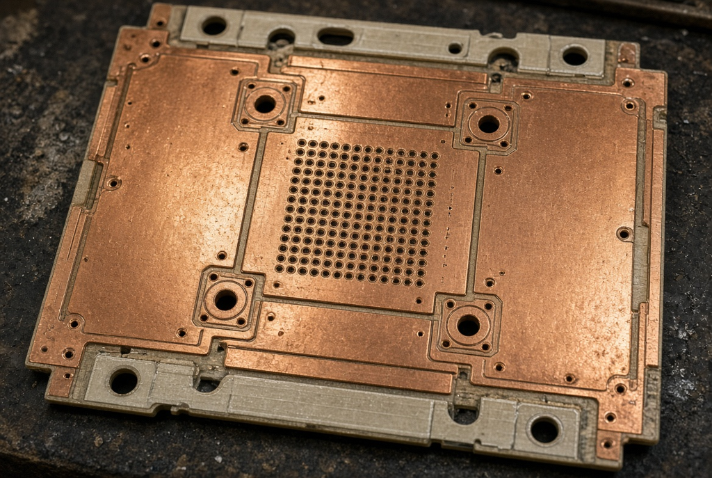
The most common method to drill through the PCB without leaving the FR-4 is to design the PCB with thermal vias. They are holes which are not intended for routing, but rather conduction. They are used in combination with a thermal pad that turns a stack of dielectric material into a collection of short copper barrels.
How Thermal Vias Reduce Through-Board Resistance
Many parallel metal paths exist from the top foil to inner planes or to the other outer foil, and are formed by an array of vias under a pad. The small conductors are each a barrel. Together, they decrease the effective resistance of the thickness of the dielectric. A spreader that is attached to the bottom or a metal insert or a heatsink footprint can transfer top-side heat.
The array will only function when both ends of the barrels meet copper that runs along. Vias that end at an inner plane that is hatched into slivers, or which emerge at the bottom of the substrate and end up in a small unobstructed pad transfer heat a few hundred microns and end. If you can’t be careless when choosing the drill size, you cannot be careless when choosing the landing layers.
Fabrication/assembly issues – filled or capped vias under a pad – are not thermal issues. Unfilled vias can suck solder out of the joint, and/or leave voids. The tradeoff for the filled and plated over via is that it makes the pad flatter and makes the path smoother for the copper, but also adds process steps. The choice of construction on a specific part should be made on package recommendation, and not the default in the CAD via template, because of what the fabricator is capable of holding.
Via Size, Count, and Fill Considerations
The smaller the drill the more barrels that go in a pad. The individual path can be a loser, and one barrel may not contain as much copper in it, but if the count gets high enough and the plating is uniform, the array can still be a winner. The larger the drill the better the conductivity, and typically the greater the size the easier it will be to plate (but it will require more space between the holes to consume in the pad, and it could cause a decrease in the thickness of the copper between holes).
In general, there are more ways to decrease resistance, until the pattern is no longer conducive to fabrication. The aspect ratio, min web between holes, annular ring on landing pad and voided via all have a max value. Once one surpasses that ceiling, or the “add ten more holes” stage comes and becomes a yield problem.
No one universal via recipe for blogging that’s a company specification. Many power components will include starting patterns in their packages. These are used as initial sketches, then the fabrication process is verified by the fabricator against the actual stack-up, for drill, plating, fill and mask openings. If the thermal budget is just sufficient to pass by geometry, or perhaps simply not enough to fail, document this in the fabrication notes, instead of a generic via tool.
Common Pitfalls in PCB Thermal Design
The three habits that produce most thermal surprises with first article are: Copper is a heat-sink, Any power density is fine with FR-4, Freeze before any user who will have to use the board sees the and/or material features.
Relying on Copper Without a Clear Heat-Rejection Path
Teams still pouring, bumping weight of copper and still getting hot spot. The copper is in good working order. The system is not. The heat is spread out over a larger surface area of foil, but there is no contact with the chassis, no footprint on the heatsink, no airflow directed towards it, no metal-core plate attached to the case.
Symptoms are consistent. The surface temperature of the board is warm and it is not at one pad. Bloom is only seen in infrared out to the edge of the pour. Further additions of copper do not alter the peak, but alter the shape of the bloom. It’s not the first ounce of foil that’s gone missing, it’s the last interface.
Prioritize that interface BEFORE layout. Here is an example thermal path: FET Q3 pad to top plane to via field to bottom copper to stamped heatsink with thermal interface specified. This is NOT “Place a copper around Q3”.
Ignoring Dielectric and Via Limits in High-Power Designs
Many converters and strings of LEDs will get a good amount of heat from standard FR-4. If the density is high enough, then the dielectric will serve as the series resistor and it is impossible to put a sufficiently large number of vias on such a laminate that wouldn’t make the board a metal plate.
It’s true to say that the PCB thermal design of power electronics is a process that should be done early in the design phase. If the product needs to pass a few millimetres of board thickness into a cold plate, it is in high thermal or metal-core territory or you will need a mechanical heatsink, not one that uses the laminate. That late-learning-the-stack-up is a costly exercise should have changed.
Over-Constraining Thermal Features Without Fabricator Input
Process windows for aggressive via field, filed via under fine pitch pads, unusual dielectric system and heavy-copper / standard-copper stack. If all the components are in a white paper, and no discussion is had, after sending the Gerbers, you get the predictable email: you can build the board, it is just not going to have all of the features or be built at that price or that schedule, or is not going to be reliable based on the drawing.
Be clear during the stack-up stage, before it is final, about the thermal reasoning. A practical via pattern can be consistently plated and filled while an ideal pattern will need to be waived. This also applies to material calls out. Better than copying a brand and thickness from a set of project notes without knowing availability, is to designate a family and the purpose for it.
Practical Thermal-Design Checklist for PCBs
This is a pre-layout pass of all parts that heat to a temperature that is of concern. It has no purpose. It’s not about acquiring the more rules, it’s about writing the path.
Define the Thermal Path Before Routing
For each high power device, write ‘4 things’ before taking the rest of the net:
- Any point of entry of heat to the board (pad, exposed slug, through-hole body).
- How it is spread (planes, thicknesses of copper you are not cutting, keep-outs etc.).
- The way it traverses the thickness (field, metal core, edge plating, mechanical boss).
- The place where the heat is released out of the assembly (heatsink, enclosure wall, directed airflow).
If one of the 4 is “undecided”, STOP and DECIDE it. The routing of the thermal path around an undecided route creates Islands and Neck-downs. Do the same four items again when the layout is “done”; plane cuts and stitching vias wander at the end of the week when releasing a layout.
Match Materials and Via Strategy to Power Density
Continuous planes and via field with an area equal to the pad area can be used for a conventional multilayer and conventional laminate for low to moderate dissipation. There must be a material conversation to be made when considering high power density, or when a product requires to operate in still air inside a small housing, higher-conductivity dielectric, metal-core or a heatsink which does not require the laminate to do the last mile.
Discuss the combination, not its individual features with the fabricator. The constraints of the others are used to limit the size, fill, copper weight and family of the substrate. The upside of the review is that this is not a temperature drop guaranteed construction, it’s a construction that is also manufactureable.
Treat PCB Thermal Resistance as a Design Variable, Not a Fixed Property
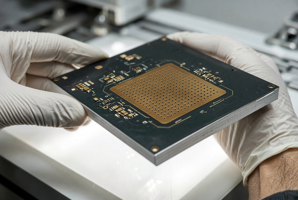
Thermal resistance of PCBs is not a specification that is included when the laminate is specified. This comes from the paths that you draw: Dielectric, copper distribution and via structures, all finished with whatever hardware rejects heat. Set that path before it is possible to change the path or stack-up. For copper use the correct size, not the size of copper that you like to draw. Also make sure to use the proper size and not a copper that you like to draw for the vias. Integrate the fabricator early – before it is ‘frozen artwork’ such as via field and material family.
Then do that work once and on paper – far less likely that first article will be the first time anyone looks to where the heat goes.