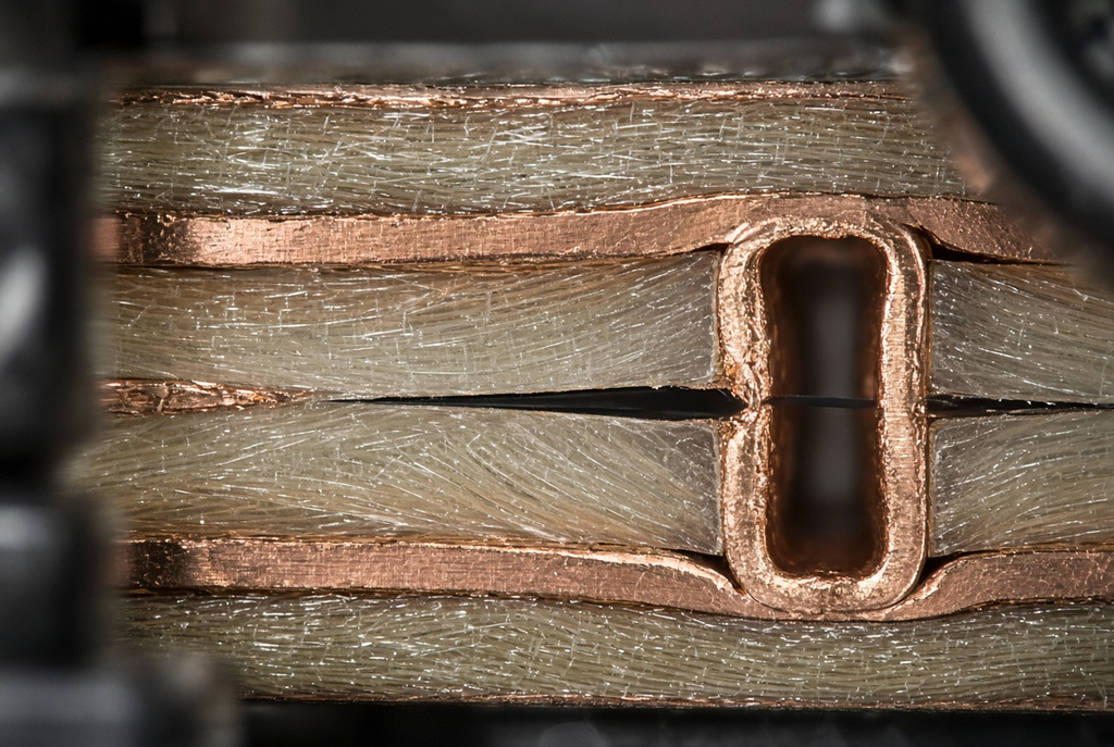
The separation of the layers within the prepreg/copper interface, core/copper interface and separation along a via is known as PCB Delamination. It can be produced in the manufacturing process, reflow or in the field and during thermal cycling. It can be only one fault, and it is rare. All of these factors play a role prior to the appearance of a blister or intermittent open in laminate: moisture in the laminate, bond quality from the press cycle, CTE mismatch in vias, stack-up balance, and the number of times the board is heated.
The easy road to take is to blame the fabricator and “one bad lot”. Risk changes due to design decisions, after shipment storage, assembly profile and rework. This guide will assist you in understanding the sources of delamination, the interpretation of the root cause, the confirmation of failure and how to minimise the risk of failure in new and existing designs.
What Is PCB Delamination and Where Does It Occur?
Delamination is like a bond failure, which means that an opening was not designed. There is a crack that air and moisture are able to get in. As that interface opens, electrical isolation (through integrity) and mechanical stiffness reduce, and sometimes, even if it takes a cycle to open, immediately and sometimes after the next thermal cycle, respectively.
Layer Separation Between Core, Prepreg, and Copper
The most frequent flaws are a separation between the core and the prepreg that was supposed to be locked to it or a separation between the copper foil and the resin that was supposed to wet and lock the copper foil. The same type of damage is observed as a lift at the inner-layer capture pad of an INAS (plated via) or as a crack along the barrel. At the skin level, blisters or an elevated area that is discolored may be observed. Internally, you may only see a thin opening or perhaps a hairline which closes when the board is warmed or flexed.
Therefore, incoming visual inspection is not a good filter. A board can be made clean, with an initial electrical test pass, and still have a bad interface that will open up in 2nd reflow and/or on a few hundred thermal cycles of product use.
Common Locations: Vias, High-Stress Areas, and Thick Multilayers
Priority sites can be predicted, if you think about the areas where stress is concentrated.
Copper and dielectrics expand at different rates for every board heating when the hole is high aspect ratio (HAR) and is in a thick construction. There, via barrel cracking and delamination is typically observed. A weak bond has more volume in which to grow in thick multilayers because they have more resin, they have more copper planes and the path of moisture and heat is longer. Mechanical load is placed upon the thermal load on areas that are under large packages, heat generating parts, connectors that are subjected to insertion force and regions on the board that are bent during the handling and depaneling process.
Start at those areas, not at random areas around the panel, when doing a failure investigation or Design Review.
Root Causes of PCB Delamination
Useful failure file isn’t restricted to “delaminated.” Identifies how the interface was opened. There are four (4) main groups of causes for PCB delamination, which tend to bundle together on a single part number.
Material and Lamination Quality Issues
The process that is supposed to make cores, prepreg and copper one bonded stack is lamination. Even though the finished board is normal, the bond line is weak if the press temperature, time or pressure is not correct, if the inner layer is not oxide or is not treated with adhesion, or if the surface is contaminated before the book is loaded. Materials can also be an issue – resin deficient glass, voids in the prepreg, inconsistent reinforcement or a lot of prepreg that was stored at conditions that were not as specified.
Most of this will be picked up by the good fabricator from incoming material control, qualified press recipes, and coupon/microsection checks. The customer will not have to develop a press cycle. It should be the viewpoint that the quality and reliability of PCB lamination should be documented and should not be assumed to be a “FR-4.” Prior to the stack-up being deposited, specify whether it is thermally or mechanically demanding.
Moisture Uptake and Pop-Corning During Reflow
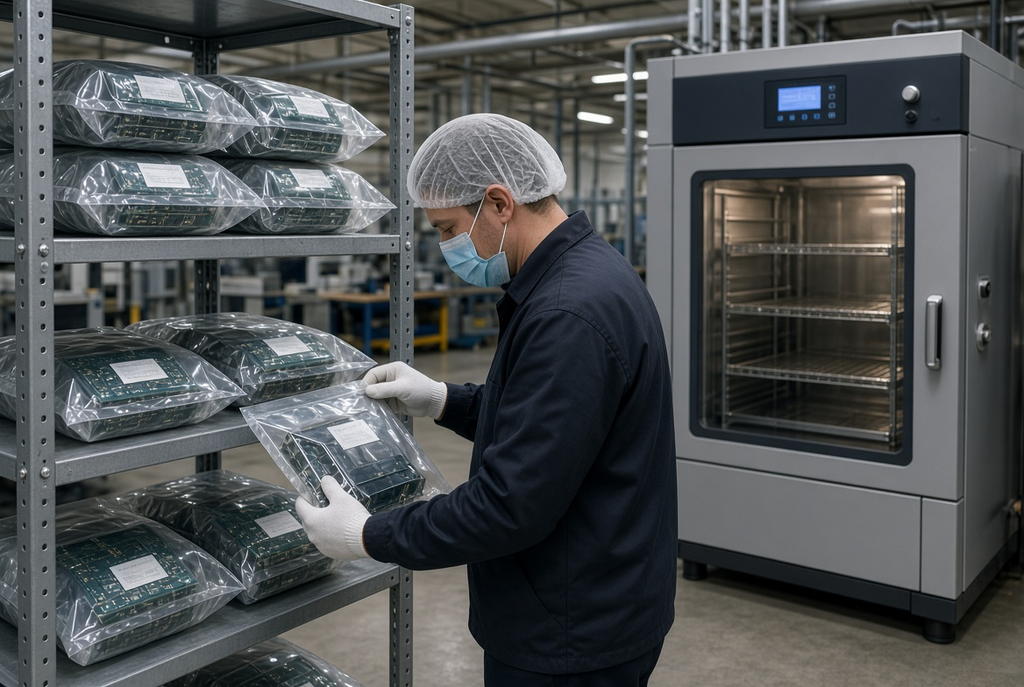
Laminates have the ability to take up moisture from air. Slowly dry room if necessary. Not in an open warehouse or after a long sea voyage, or after weeks in an open package. That moisture is more volatile than evaporating at reflow. The weak interface is then pushed up due to the pressure from the inside. The dramatic version is called “pop-corning” and the quieter version is “moisture-induced PCB delamination”, which is not discovered until after 2 or 3 heat cycles as a blister.
The risk increases with thicker boards, higher resin content constructions, higher profile materials, and with multiple reflows/reworks. Not all prototypes require baking, but when the board is moisture sensitive, the profile is aggressive, or the storage history is questionable, then baking is a true control.
Thermal Mismatch and CTE Effects in Vias and Multilayers
The rate of expansion of copper, resin and glass are not the same. It is important to understand glass transition temperature (Tg) because above Tg, the resin’s expansion increases significantly in the Z-axis. Then each reflow, each wave or each field temp swing pushes the plated barrel against the dielectric. Over time this stress will result in the interface or copper opening or cracking. Copper peels off the edge of a large plane due to the same mismatch causing a stack-up that is out of balance.
This is why the material class for a two layer consumer board might not work for a thick multiplayer, located near a power stage or outside. Association of material family with via structure to actual thermal environment, not lowest cost default stack-up.
Excessive Rework, Mechanical Stress, and Handling Damage
Close to the extremes of temperature and/or mechanical strength, a design does not need a severe insult. Cracks starting during a second hot air BGA installation, flexing a board to fit a connector, de-panneling too close to a via field, or stacking bare boards on edge can all lead to a crack starting that may seem to be a “mystery” field failure. The issue becomes worse when there are several reflow processes without moisture control.
If you are using the “until it works” approach for your NPI plan, then include the rework limit in the process before the 1st article return, instead of after the 3rd article return.
Detection Methods for PCB Delamination
There is a distinction between suspicion and confirmation. A visual/visual symptom can help you determine what corner of the board you’re viewing.Visual/visual symptom may help you know which corner of the board you are looking at. Don’t expect them to close the file automatically.
Visual Inspection and Electrical Testing Clues
The severe case is when the blisters appearing on the solder mask, the solder mask is raised, the solder mask is discolored or is lifted at a hole and/or edge. There aren’t many real failures that don’t. Electrical test can cause an open or intermittent open after thermal cycling or can cause the resistance to increase on the via net. Their findings show that the track had altered. They are not a sign of a barrel cracking or a pad lift caused by a pad cratering or other solder joint problem; they are just a sign of delamination.
Cross-Sectioning, Microsection Analysis, and SAT
A course that provides cross-sectioning, microsection analysis, and SAT training.
The interface is still considered destructive work. Taking a microsection of the suspect via or blister will show whether the split is core to pre-preg or under the foil or in the barrel. It is also possible to see the thickness of the residual copper, folds in the copper plating, as well as the areas where copper was first applied (in a resin rich pocket or on the pad corner).
The common counterpart usually used with the laser is scanning acoustic tomography (SAT) or scanning acoustic microscopy (SAM). It is beneficial if only a few samples, or consider unit sectioning. No microsection and SAT for delamination should be considered as default screenings to be performed in each and every production lot. They are meant to be used for failure analysis, incoming dispute work or qualification of a new stack-up or new assembly profile.

Prevention Strategies Across Design, Fabrication, and Assembly
There is no one simple process change to prevent PCB delamination. It’s a collection of choices that have to conform to one another.
Design-Level Prevention: Stack-Up, Vias, and Material Class
To ensure good press/reflow interface, use a balanced stack up (otherwise copper will accumulate a warp). A routing decision is not a thermal or routing limit of via aspects, a very small hole through a thick board is a reliability decision, not a routing decision. Select material class which has suitable Tg, decomposition characteristics and moisture characteristics for the profile of the assembly and environment of use.
Do not assume the layout is finished until you have some parts frozen with a stack-up and a via plan with the fabricator and are certain that they are high-reliability or high-layer count parts. It can be easily changed after quotation, and it becomes a “high stress” construction, if the hole size or adding planes are changed in a “standard” construction.
Fabrication Controls: Lamination Process and Material Handling
The most crucial aspect of the factory side is the qualification of the lamination recipes, the storage of the drying and clean material, the preparation of the inner layers that are actually measured and the coupons, which serve as a representation of the book that is to be sent to printing. Using laminate lot to finished panel tracking, you can simply contain the problem without getting embroiled in the issue.
Communicate reliability intent early – operating temp range, number of assembly heat cycles, or whether it is expected to be subjected to heat cycling in the field or not. A fabricator can’t apply the right process window if he is not there.
Assembly and Field Practices: Moisture Control, Reflow Profiles, and Rework Limits
After the board is in storage, it’s under the threat of heat and danger. Until line is ready, keep moisture barrier packaging. The rules must be written when the package has been opened, when the board is really thick, or the product is ‘moisture-sensitive’ and baking is not done unless the rules are written and not based on the tribal’s habit. Use a safe-to-laminate, safe-to-component profile – chasing a colder profile that is not completing the solder joints is not a delamination strategy.
Cap rework. More heat cycles allow more moisture to be extracted and CTE stress to finish the crack that might have been opened in the first heat cycle. However, it also has its own significance in the field; don’t use a completed assembly as a pry bar when a connector jams.
A Practical Delamination Risk-Reduction Checklist
For new designs use as a review sheet, for failure sheets use as the first page. The answer does not necessarily have to be “elegant. These ought to be documented.
Design and Material Selection Checks
- Are the material class and operating temperature right for the assembly profile planned (with the possibility of a second side reflow)?
- Are large planes on one side of the midplane or is the stack-up balanced?
- Have a reasonable via aspect or asking a small hole to cross a thick structure?
- Are aggressive scoring on large packages or connectors, or heavy copper, board edges been given additional clearance from high stress areas, and do vias have enough clearance under mechanical load?
- Can the number of reflow, wave, selective or rework heat cycles be seen by both the designer and the fabricator?
Fabrication and Assembly Process Checks
- Does the fabricator have a lamination process documented and a method to track lamination lots to the panels that you received?
- Are bare boards stored/moisture proofed in shipment and installation?
- Is there a written procedure for package break, dwell time and/or moisture sensitivity of the building?
- Are the reflow profiles aware of the class of the laminate for which they are being used or are they copied from another product that is not related to the laminate?
- Are there high reliability or thermally critical assemblies with a rework limit and do they respect that rework limit on the line?
Summary Guidance – Treat Delamination as a Preventable System Risk
The delamination of PCB is not a property of multilayer boards, it can be prevented as a system risk. If design, material, press quality and moisture-heat are not in harmony, the interface does not work. Detection Methods: Describes which of the interfaces was opened. Prevention is the activity of ensuring those five inputs agree prior to the first production lot, and maintaining the agreement throughout the remainder of the production process (storage/rework).
On the next new stack-up, on the next board which will return with a blister or an intermittent via: use the locations, root-cause groups, checklist above. The goal is NOT to assure a no failure! The aim is to develop a design and process that don’t come as a surprise when it comes to delamination.