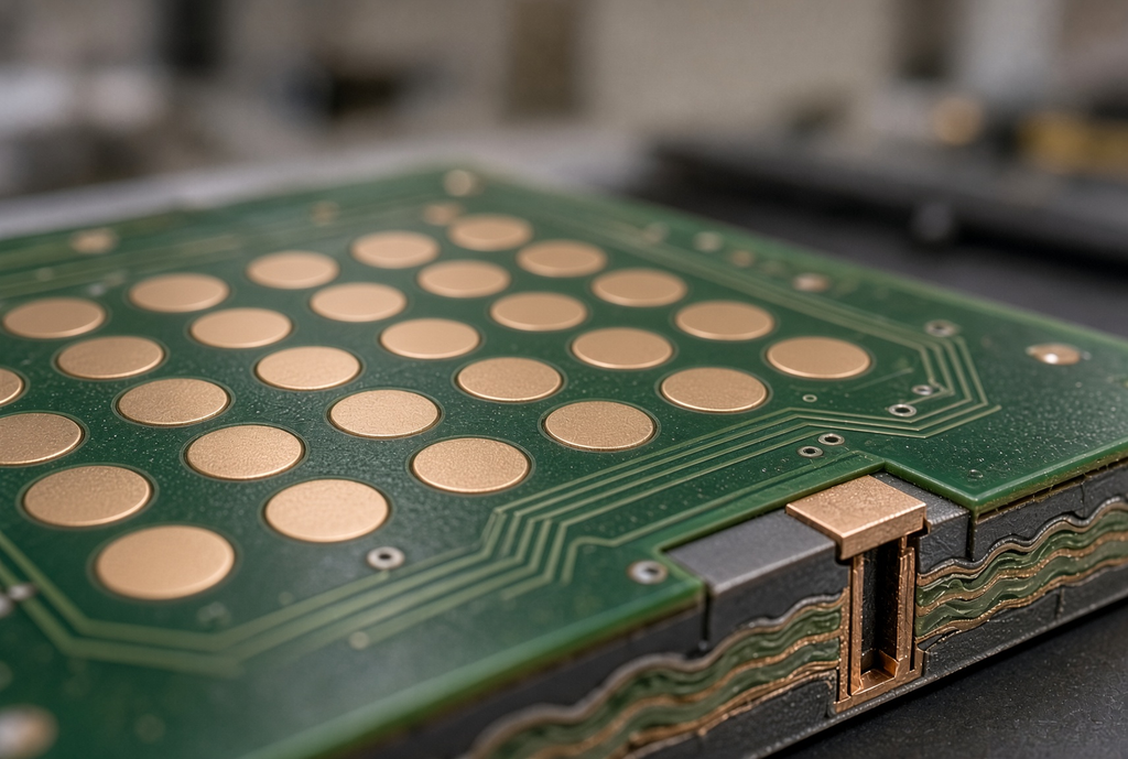
Via-in-Pad Technology: Design, Filling, Plating, and Assembly Considerations
A practical guide for PCB designers, hardware engineers, and layout engineers who need to use via-in-pad on fine-pitch packages. It clears up when via-in-pad beats traditional fan-out, how filled versus unfilled and conductive versus non-conductive fill change the land, and what to write on fabrication and assembly notes so plating, capping, stencil design, and reflow stay aligned.
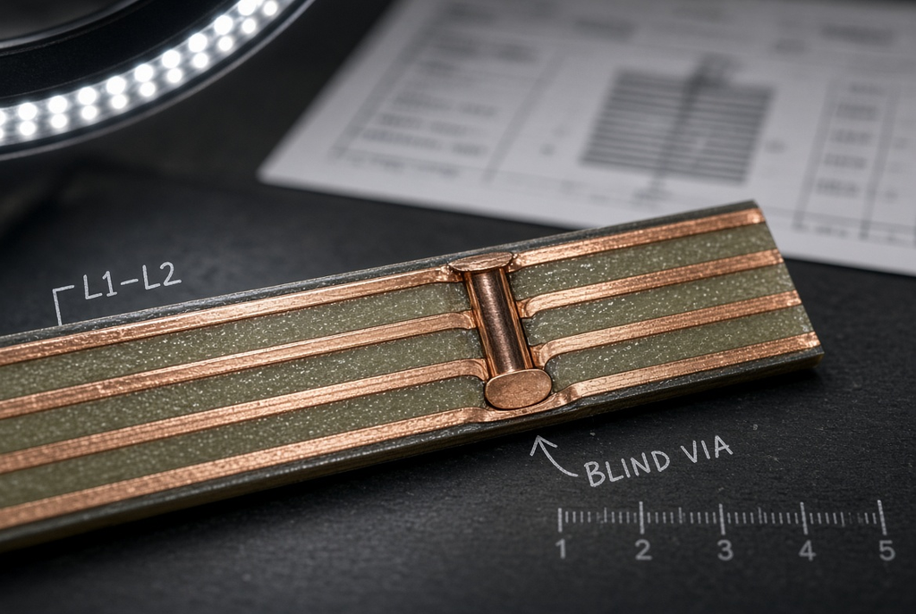
What Is a Blind Via? Structure, Benefits, Limitations, and HDI Applications
A practical guide for PCB designers, hardware engineers, and layout engineers who need to separate a real density problem from an HDI label. It explains blind via structure, layer-pair notes, routing and signal-integrity trade-offs, and fabrication limits so you can decide when a blind via belongs in the stack-up—and how to write it so the shop does not guess.
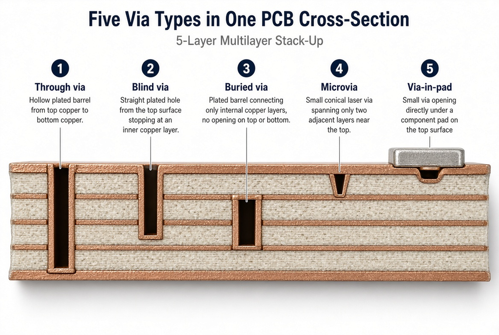
What Is a Via in PCB Design? Through, Blind, Buried, Microvia, and Via-in-Pad Types
This guide is for PCB designers, hardware engineers, and buyers who must choose a via structure before releasing files. It explains what a via does, compares through, blind, buried, microvia, and via-in-pad constructions, and ties each option to routing density, BGA escape, signal behavior, assembly risk, and fabrication complexity so teams can specify the simplest build that works.
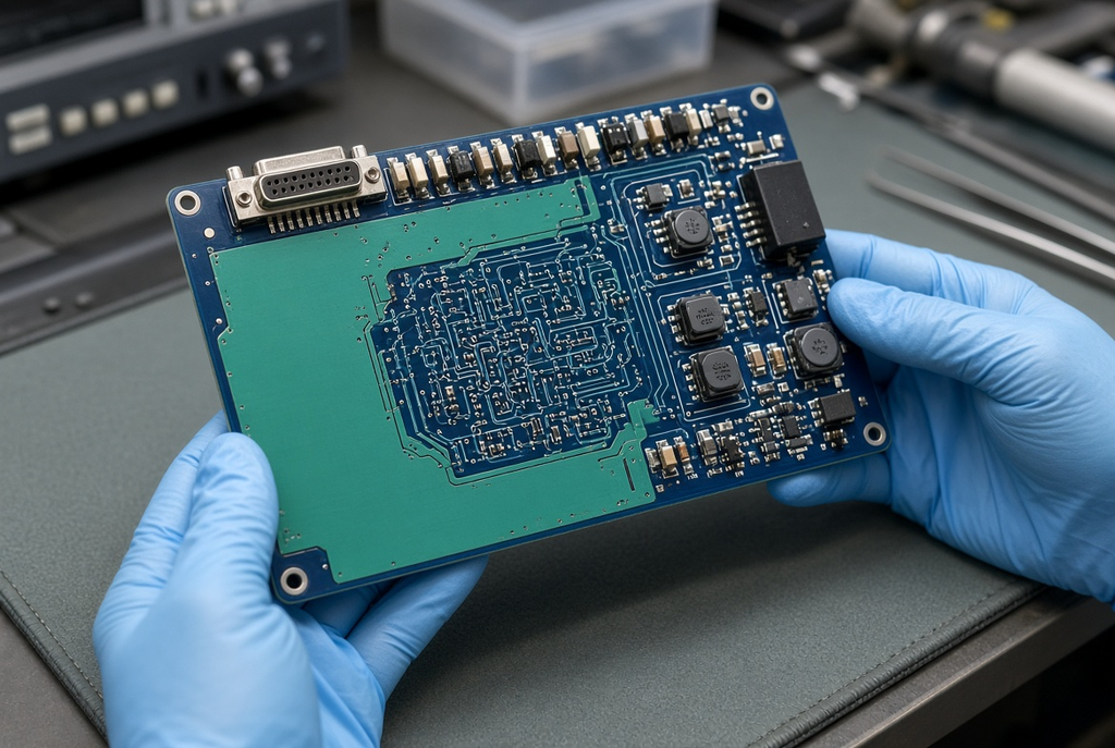
EMI PCB Design Guidelines: Layout, Grounding, Stack-Up, and Filtering
This guide is for PCB designers, hardware engineers, and EMC engineers who need EMI control at the board level—not last-minute filters before a test house visit. It explains how stack-up, grounding, return paths, partitioning, and interface filtering work together, and what to write on fabrication drawings so the built board matches the EMC intent.
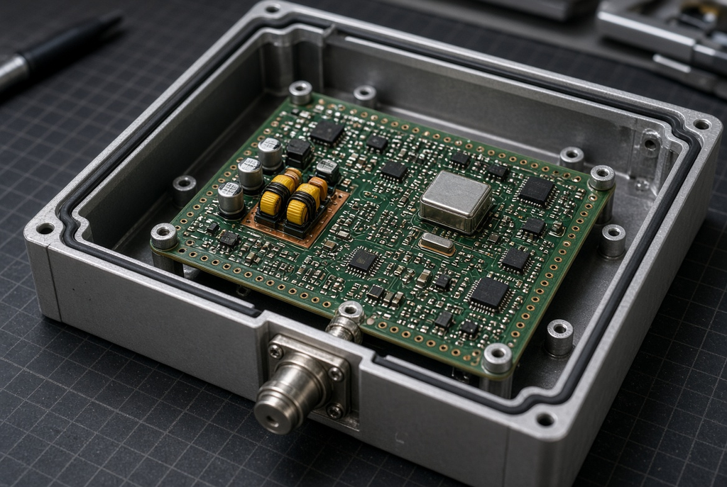
PCB Shielding Explained: Methods for Reducing EMI and Signal Interference
This guide is for PCB designers, hardware engineers, and EMC engineers who need signal interference reduction at the board, not a field-theory overview. It separates board-level shielding from enclosure shielding, then walks through ground planes, copper pours, local cans, stack-up choices, and the fabrication notes that keep CAM and assembly from guessing.
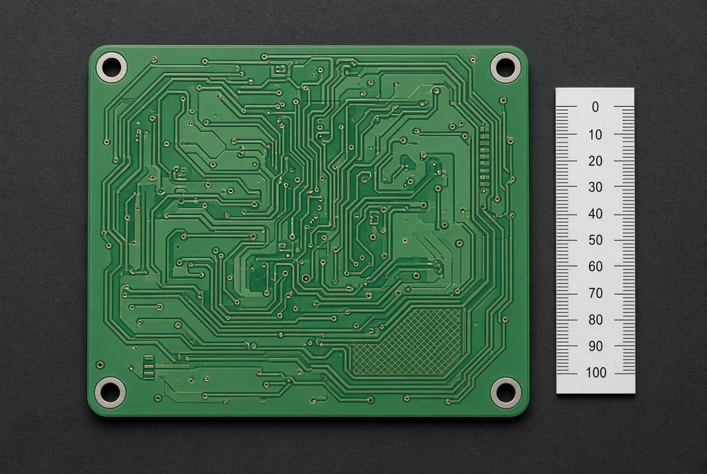
PCB Traces Explained: Width, Spacing, Thickness, and Routing Basics
A practical guide for PCB designers, hardware engineers, and layout engineers who need to set trace width, spacing, copper thickness, and routing without guessing. It explains drawn versus finished geometry, inner versus outer etch, and how to write fabrication notes so impedance, current, and yield stay aligned.