PCB shielding refers to a group of techniques and procedures that is implemented for board-level and mechanical containment of electromagnetic energy, and for reduction of coupling into quiet circuits. It is not a metal can that fell on a loud track because of the first poor EMC result.It’s not a metal can that fell on a loud track after the first bad EMC test. Shielding is only effective where return paths, stack-up, partitioning, filtering and enclosure grounding provide already a controlled return path for currents, as in a mixed-signal board, a switching supply and a high speed digital design.
A shield does not fix a slotted ground plane, a node connected to a switching analog input, or a two-layer board that has no continuous reference. The assumptions you made manifest themselves as radiated emissions, a noisy front end, unstable high speed links, and a re-spin that a can never could have avoided.
What “PCB Shielding” Actually Means in Practice
PCB shielding is not a single part number in production language. It is a mix of reference planes, copper strategy, local metal and the manner the board sticks to the case. EMI shielding is done on the surface of the board and PCB assembly shielding is done on the surface of the enclosure. Here’s how a team can purchase a can and go out of the chamber.
Board-Level Shielding vs Enclosure-Level Shielding
The Board-level shielding resides in the stack-up and the copper. This includes solid ground and reference planes, a copper pour for shielding around a noisy island, stitching vias that close the copper pour to the plane, guard traces between a clock and a sensitive net, and a local shield fence or can soldered to a grounded pad ring. Their role is to minimize the return loops, couple the sections less, provide a metal return path to the high frequency current but not the air.
Enclosure level shielding is the metal case, conductive gasket, connector shell and chassis bond. A good enclosure minimizes the aperture radiating, and provides a low-impedance termination point for cable shields. It does not create a return path which the PCB never did.
The practical dilemma, however, is well described. The aluminum housing is shared by two products. One board has a continuous ground under the switcher and the analog section, and the connector shells are attached to this plane at the entry. The other board is a two-layer pour with thermal-relief islands and the other board hopes the box will cover up the loop. No enclosure shielding can close a loop, if one already exists on the laminate.
Shielding as Part of a Complete EMC Strategy
Imagine two boards with four layers each are going into the same radiated-emission test. Board A stays in its own area, puts that area on top of a solid ground, pours that area, and filters out the cables at the connector. A shielding can and a ground are laid on the copper on the Board B over the converter, but the ground is cut by a connector slot and the analog return is cut as well. Same enclosure. Each plot, rework, and sometimes the cost after someone has to open the can and move a trace and spin the board.
Shielding is just one part of an overall EMC strategy – controlled returns first, partitioning and filtering second, local metal third, case fourth. The sequence is the PCB layout for EMC. The opening line is the first sentence in that sequence, not the can.
Core PCB Shielding Methods for EMI and Signal Interference
None of the methods outlined below are standalone. Signal interference reduction is achieved by stacking them in the design order: planes & returns, followed by copper & partitioning, followed by a local can with layout still needing a lid.
Ground Planes and Reference Planes as the First Line of Defense
Most boards already pay for a ground plane for EMI. A continuous reference under fast or steep edge will follow the signal path and not wander across the board and radiate. If the plane is split without defining a bridge, the return is the long way around the split to “keep analog clean”. The long way is an antenna.
Continuity is more important than copper weight slogans on board a plane. Typically, a thin, continuous signal layer next to the ground layer is more effective than a thick layer (diced with slots, unstitched thermal reliefs and connector cutouts). These values of via pitch, plane-to-signal spacing and stitch density are guidelines and should be verified with the stack-up, the edge rate and the ability of the fabricator to be able to etch and plate on that construction.
| Ground planes as the primary shield | What breaks the shield |
| Continuous reference under noisy and quiet circuits so return current stays under the trace | Slots and connector cutouts that force the return around an opening |
| Adjacent ground next to a high-speed or switched layer, so the loop area stays small | A two-layer board with no continuous ground, plus a can added “to fix EMC” |
| Stitched pours and via fences that tie local copper back to the reference plane | Thermal-relief spokes that isolate a pour or can pad from the plane at RF |
| A single, documented reference for impedance-controlled nets | Impedance calculated to layer 2 ground while the note or Gerber implies a different plane |
| Quiet analog and noisy switcher sharing a plane only at a planned, short bridge | A decorative split that looks tidy in CAD and becomes a slot antenna in the chamber |
Local Copper Pours, Guard Traces, and Partitioning
When a section has tone that is too loud or too delicate, local copper is beneficial when the rest of the board shouldn’t share that tone. Shielding of copper around a DC-DC island, crystal or front-end (RF) of a power supply lowers the amount of open copper surface that can couple. The only assistance that guard traces between a clock and an analog input can provide is if both ends of the guard are connected to the same quiet reference. A floating guard is just another coupled conductor.
Do not partition on a CAD tool (part of the tool is not enough). Maintain short and local node switches. Do not cross under those nodes with analog returns. Attach the pour at a regular spacing around the island, which will make the pour a part of the plane, not a floating plate. This isn’t a comprehensive high speed routing class. It is the most basic copper discipline which makes later EMI shielding less expensive.
Shielding Cans and On-Board Metal Shields
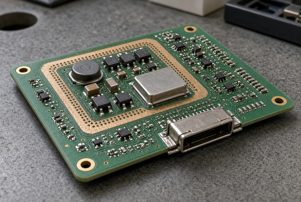
On RF front-ends, noisy oscillators and small size converters with tight coupling, a shielding can on PCB copper works strong numbers. The can must have a grounded continuous pad ring, sufficient number of stitch vias underneath the pad ring and keep-outs, where the part can be placed and soldered. Cans increase height, pick-and-place or hand assembly step, inspection access issues and cost. They must not cover a broken return layout.
Never consider can size, fence height or assembly techniques as a factory limit. Those are project notes, part number, pad ring, keep-out, and can soldered, clip-on, fence-plus-lid.
Stack-Up and Layout Choices That Make Shielding More Effective
Proceed with the decision in designer fashion: stack-up, return paths, partitioning, local shields and then enclosure. Do not use a shield as a reference plane, or as a good routing.
Stack-Up Strategies That Support Shielding and Controlled Return Paths
ssign a ground to high-speed and switched layers next to them. Do not use orientation (or “Z”) control nets in the calculation. Separate noisy and quiet portions of sound within the same layer pair, don’t rely on an inner layer pair to remove unwanted noise from a messy top layer pair. A typical mistake is a two-layer board that has no continuous ground, a dense pour that is more of an island, and a late request for a can. The can is placed on a board without any shield in the copper.
When Local Shields and Enclosure Integration Are Justified
Local metal is typically added to high-speed digital edges, RF, and switching power sections or to consider enclosure grounding seriously. Those requests aren’t the same as “please give us a clean four-layer stack-up.” A bond between a bondable part (a can) and a chassis requires that there be a plane on the board to which the can can bond and a footprint on the connector to which the shell can bond.
Heavier outer copper, large pours aid in current and heat, and change etch, spacing, registration, soldermask. That’s a made up conversation, not an automatic EMC upgrade. Copper weight is not a published maximum weight. You can write the final copper that you want and have the fabricator verify the build.
What Gets Harder as Shielding and Copper Density Increase
The higher the copper density, the less comfortable it is, typically.Typically, the higher the copper, the less comfortable the minimum space, soldermask dams and impedance tolerance. A purchasing lead should have questions when a fine pitch footprint is adjacent to a large ground pour or shield keep-out. Thermal vias and metal-core boards conduct heat in a different way and not an additional EMI shield.
How to Specify Shielding-Related Features So Fabrication and Assembly Do Not Guess
The note you will write is what CAM and assembly will create, not what you intended when you went into the review call. For any impedance model, at least identify the plane layers, pour and stitch rules, shield keep-outs and reference planes. For builds for which an IPC acceptability class is relevant, state the class name. There is no such thing as a class called “standard shielding.There is no such thing as a process called “standard shielding.
Callout Matrix for Shielding and Grounding Fabrication Data
| Write this in the fabrication data | Do not leave it implied |
| Ground and reference plane layers by layer number and function (for example, L2 GND, L5 GND) | “Ground as needed” or a stack-up PDF that disagrees with the Gerbers |
| Copper-pour connectivity and stitching-via requirements (net, via size class, and that the pour must not float) | A pour that looks solid in the viewer but is isolated by thermal reliefs |
| Shield keep-out and keep-in areas, pad-ring net, and whether a can or fence is installed at assembly | A silkscreen rectangle with no copper ring and no assembly note |
| Impedance-model reference planes that match the controlled-impedance table | Impedance called out to a plane that the stack-up does not provide |
| IPC acceptability class only if the purchase order and drawing require it | The phrase “standard shielding” with no class and no inspection note |
| Copper-to-edge clearance and heavy-pour or heavy-copper notes that affect etch and soldermask dams | A dense pour drawn to the outline with no edge or mask note |
Where the Shielding and Grounding Note Should Live
Place the note on the stack-up as well as the fabrication drawing and maintain the same revision for Gerbers, drawing and order record. A frequent mistake is a Gerber set that doesn’t contain a plane note or a stack-up PDF that contains an instruction to “ground on layer 2” when the portal field still reads “2-layer board.” The can has no pad-ring net when it is given to Assembly. The entire purpose of the paperwork is one controlled note and a revision when the plane, pour or can changes.
Cost and Yield Effects of Shielding That Do Not Show Up in the CAD Tool
Heavier copper and large pours increase the cost of foil and etch time, and increase risk of not getting a yield on a fine space adjacent to a pour and/or a shield keep-out. If the first stack-up never returned to the chamber, they can avoid a spin. Only compare quotes after taking into consideration that all copper, all layers and the minimum space are the same for each line. Price, capacity, and lead time aren’t part of a design article; they’re on the quotation for that job.
Frequently Asked Questions
Is a shielding can enough to fix EMI on a poorly laid-out board?
No. If the partition and the return path are already sane, then A can contain a local source after it’s returned. It cannot be used in place of a missing ground plane, close a slot under the can, or prevent a cable from radiating if the cable connector shell has no place to attach to.
What is the difference between board-level shielding and enclosure shielding?
Board-level shielding is planes, pours, stitch vias, guards and local metal on the PCB. The case, gasket & connector-to-chassis bond is the enclosure shielding. They stack. This case is not introducing a return path that the laminate never had.
Should every layer use a solid ground plane for shielding?
No. Each layer with a fast switch must have a reference nearby. Thickening and adding capacitance (plane to plane) and cost are added with extra solid grounds but without fixing a poor partition on the signal layers. Place the ground location of the return current.
Does more copper always mean better EMI performance?
No. Unbroken reference copper assists. High aspect ratio fine features can be surrounded by wider spaces due to isolated heavy pours, unstitched thermal reliefs, and copper that compels wider spaces in the fine features, making etch and yield more difficult without sacrificing the loop that actually radiates.
How should shielding and grounding be written on a fabrication drawing?
Label the plane layers, pour connectivity and stitch rules, shield keep-out and pad-ring net, impedance reference planes, etc., as determined by the order in which they are needed. Do not put that note in email, keep it on the drawing and the stack-up.
When is a shielded enclosure the right question, rather than changing the PCB stack-up?
Request the enclosure after the board is already covered with a continuous reference and sensible partitioning and cables, apertures, chassis bonds are the remaining emitters. If the board remains a two dimensional patchwork and has no plans for return, alter the stack-up first. That won’t be done by the box.