EMI PCB design guidelines begin with the stack-up and the layout and not in the test chamber. Reference planes, return paths, adjacent noisy and sensitive parts, and cables leaving the board as antennas determine the level of radiated emissions, susceptibility, and a significant amount of signal-integrity problems. Filtering and shielding preserve the cleanliness of a clean board. They are not considered to be an alternate ground plane.
The common misconception is: “the filter and the can will make a noisy board.” A design where clocks are routed over splits, park switching nodes are adjacent to analog and connectors are not treated still fails, or passes only after a respin. In this guide, layout, grounding, stack-up and filtering are considered as one system, and what to write on the fabrication drawing to ensure that the built board is in line with the intention of the EMC.
What “EMI PCB Design” Actually Means in Practice
EMI control is not an independent field that can be tackled after routing is complete at board level. It’s a collection of decisions that determine where the current returns, which copper is used as the reference plane, which nets can radiate and which interfaces need to be quiet before they go into the product. They appear as stack-up, grounding, layout and filtering. If one of them is allowed to be a “optional” the other(s) have to make more effort and will generally not be able to.
Signal integrity and susceptibility have the same physics as emissions. If a clock does not have a continuous return path underneath it, then it’s a victim, as well as a radiator. A switching regulator with a large area radiates noise around the analog and out of the cable saddles that are connected to the switching power supply enclosure. The reason for failing in mixed signal PCB EMI design is the same as that of the high speed link: The current you draw on the schematic is not the current that closed on the board.
Stack-Up and Grounding as the Backbone of EMI Control
The reference planes, impedance layers and physical separation of noisy and quiet copper are defined by stack-up. Grounding refers to the manner in which return current can flow and the location where return current must not “jump.” They are the backbone in combination. On top of them are layout and filtering.
Two of those layers are unconstrained signal layers and there’s no continuous ground, which is a typical first step in further EMC torment. Leftover copper poured into the ground is not a plane. Current is rerouted to the next available avenue which is usually across a split, through a via that is too open or out through a cable that has not been bonded. At that stage filtering is addressing the symptom. The “radiator” is the loop you created in the stack-up.
Typically, an EMI aware PCB stack-up will place a solid reference plane next to every fast, noisy signal layer on the PCB, will keep power and ground close together where decoupling requires a tight loop, and will not have a clock layer directly connected to a switching-power pour without adding any isolation. If the ground is to be continuous under the nets who need it, then “GND” on the drawing must be continuous on the plane that needs it; and if any part is intended to be split, it must be noted on the drawing so that the routing does not go through it by accident.
Layout and Filtering as the Second Line of Defense
Two boards can have the same number of layers, but yield different chamber results. One maintains analog, digital and power in distinct blocks, short runs clocks over solid reference and places filters at connectors. The other snakes a 25 MHz clock across a plane gap and shares a connector pin field with a switching node and a sensor input with no filtering of the I/O; “the enclosure will handle it.” Same staking in paper. Various loop zones, various coupling and various rework.
Be aware that PCB EMI layout and filtering is not a substitute for a good stack-up, it is a complement. A ferrite is not going to reduce a clock loop which is already half the board. A common mode choke at a USB connector cannot put the return path back together if it was broken by a gap in the ground plane. Filtering should be applied at nodes that have residual energy after the layout is cleaned and is located at the interfaces. It is not the design method, but rather, the second line of defense.
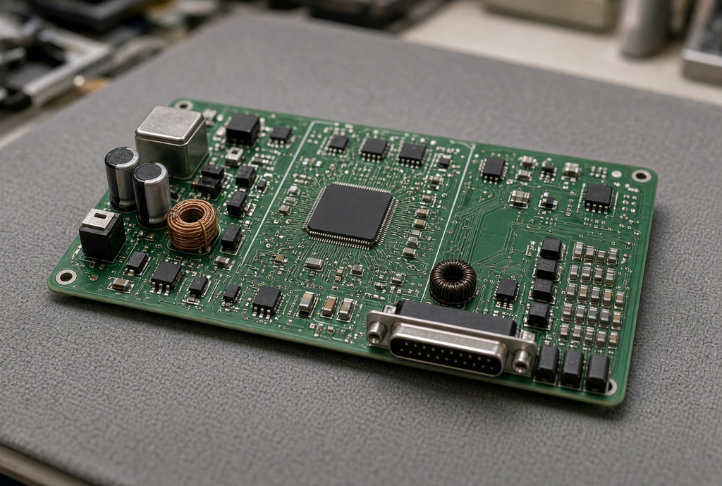
Core EMI PCB Design Guidelines for Layout and Grounding
The mechanical envelope around the board, stack-up and layout are all part of a good EMC practice. There is no “magic trick” that can be used to replace a controlled return path, whether fenced, a bead on every I/O, or hatched pour. The approaches listed below are applied in conjunction with each other. The values stated are guidelines and should be verified based on the actual stack-up, the fabricator’s process window and the product’s EMC Plan. The levels are not process limits of any single manufacturer.
Grounding Strategies That Support Controlled Return Paths
The art of providing a definite, low-current path and clearly visible grounding point for every fast or noisy current is called PCB grounding for EMI. A solid ground plane under high speed and switching nets is the default setting. When these nets split, it compels them to come back to detour, and the detour is the loop radiating.
When choosing the location for planes to open, think of this picture the following way:
| What the layout does | What happens to the return current | Typical EMI result |
| Continuous ground under clocks, differential pairs, and switch nodes | Return stays under the forward path; loop area stays small | Lower radiated emission from those nets; cleaner SI on the same traces |
| Slot, split, or isolated island under a fast net | Return jumps the gap through the nearest stitch, connector, or cable | Larger loop, stronger common-mode current, chamber failures that look like “the cable” |
| Ground pours on signal layers with no via stitching to the plane | Pour looks like ground in CAD and behaves like a floating patch at RF | Unexpected resonances; analog sections that pick up digital edges |
| Multiple “grounds” tied at a single point far from the noise source | Return is forced through that star point even when a plane exists | Star-ground thinking on a multilayer board; mixed-signal noise that follows the tie |
| Connector shield or chassis pin with no local bond to the board reference | Cable becomes the return | Strong common-mode on the harness; shielding in the box cannot finish the job |
The return path is almost always broken by some space the current wasn’t prepared to occupy: a gap in the plane for “analog isolation”, a line of unstitched thermal reliefs that make up a slot, a plain broken open by a connector, or a via fence that is not dense enough to seem like a wall at the frequency of interest. There is still a need for isolation, for instance between a dirty power stage and a microvolt front-end, but the isolation needs to be drawn so that the returns do not have to pass through the quiet region on their way home.
When you have to divide a plane, divide it on purpose. Install split where there is no fast net traversal, install analog-digital interface on nets that do cross (ADCs, isolators, filtered power), and stitch around the crossing to get a local return. A split without a crossing plan is not a mixed-signal hygiene. It is an antenna slot.
Partitioning Noisy and Sensitive Sections Without Over-Complicating the Board
Partitioning is not about ground islands, it is about floorplanning. A choice of power, high speed digital and sensitive analog or radio frequency will each require its own plot and its own neighborhood of connectors. They are not each interested in a floating ground that meets a system at only one via.
Work with blocks that have a purpose. The switching regulator and its hot loop should be in one corner, while the inductor, switch node and input capacitor should be grouped tightly together. Place clocks and high speed buses in second block, over continuous reference, with shortest possible run, but still conserving timing. Separate analog and RF from both; separate local decoupling, and don’t walk through switch node to get to a connector with I/O.
As much work as pours is required for connector placement. Either those domains are separate, or they are not, as the single connector that combines an unfiltered switching output, a crystal reference and a sensor input will couple them no matter how they are separated out on the silkscreen. Group noisy I/O, quiet I/O and the filter components together and position them at the connector they’re intended for, rather than three centimeters in, where the trace is already a radiator.
Broadband devices like clocks and switching nodes are special cases that warrant special attention. If possible, do not send them down the edge of the board. Never run them parallel to the analog inputs. Avoid just another “net” on a layer that has no reference. In that floorplan, before the first filter footprint, the win or lose of mixed-signal PCB EMI design is typically determined.
Routing Practices That Reduce Coupling and Radiated Emissions
The high-speed PCB routing guidelines for EMI are not as long as most style guides suggest. Do not separate forward and return path. Do not make the loop too large. Do not allow the aggressor to be near the victim.
Clocks and other single ended fast edges should be short, on a layer that is next to a solid reference and away from plane splits. When the clock has to be shifted to a new layer, the return must find a nearby stitch so that the current does not wander to the next visible via three centimeters away. Differential pairs should remain connected together and to their reference, and if they are tightly coupled and sent over a slot, they will still radiate as a pair of interrupted returns.
Switching nodes are layout objects, NOT schematic nets. There is a hot loop between the switch FET and the inductor and the input capacitor. Reduce that area as much as possible first of all. Snubbers and beads can be used to control what is left, but not to reduce a loop created at the board size.
Simpler, direct paths over hard reference planes are more effective at reducing EMI than a late package of filters. Filtering should be added to a route that is already quiet enough to be filtered. Don’t publish/assume a universal max trace length. Length, rise time and the “stack-up” around the net combine to set the risk, and these numbers are part of the design and not a generic rule table.
Stack-Up Choices That Make EMI Control Easier
Stack-up for EMI control is a series of decisions: How many layers? Reference planes? Controlled impedance layers? Partitioning and filtering on the stack-up? A filter should never be used in place of a good reference plane. These extra layers cannot be used as a replacement for a continuous ground that the fast nets can use.
Stack-Up Strategies That Support EMI, Impedance, and Manufacturability
The placement of a solid ground (or a well-decoupled plane) adjacent to every layer carrying fast or noisy signals is a practical EMI-aware stackup. For controlled-impedance layers, reference planes for the calculation must be named. They must be in the note, and in the Gerbers, as continuous copper, not as “leftover pour.
It is easier to separate noisy sections from quiet sections when there is one continuous reference to cover the board lengthwise, as provided by the stack-up. A frequent error is to add layers without adding that reference: a six-layer board having four signal layers and two fragmented planes could radiate more than a four-layer board having two solid references. Another problem is to install a high-speed signal layer next to a switching-power pour that is not separated by a plane. The stack-up then is a coupling structure.
This is where manufacturability should be discussed. The EMI goals must be accompanied by tight impedance, thin dielectrics and high via fields if the fabricator can control the dielectrics and registration. Record the stack-up as a construction not as a layer count on a quote form.
When Additional Layers or Heavier Copper Are Justified for EMI and Power
Layers and copper weight are typically added when high-speed digital, RF, and switching power are the usual reasons. Additional layers are available for use when specific reference planes, power-pour-heterodoubled analog layers, or impedance layers which cannot share space with power pours are needed. Heavier copper is needed when the problem is power current and thermal drop on the planes – return impedance at DC and at the switching edge, not “more copper equals less EMI” – it doesn’t exist.
Those 2 requests are not the same. A “clean” stack-up of 1 oz planes and continuous ground will out-split a heavier board that also hits the reference under the clocks. Two-ounce copper and large pours also alter the fabrication landscape: increased etch time, increased workable space, increased stress on registration, closer soldermask dams around fine features adjacent to a pour. Identify starting and finished copper and identify the layers that have the additional weight. Don’t assume that thicker foil is an EMI upgrade.
What Gets Harder as Stack-Up Complexity and Copper Density Increase
The more features that are free in CAD, the more uncomfortable they will be in the press and the more copper weight they will have, the more layers they have, and the higher density they will have. Explicit note is required for minimum space next to large ground pour, soldermask dams between a fine-pitch footprint and a heavy plane, impedance tolerance on a thin dielectric. A purchasing lead should anticipate that the fabricator will push back on a fine-pitch package against a large pour or a keep-out that the plane can’t meet.
Thermal vias and metal-core constructions are different heat paths. They have the ability to alter the power stage dumping heat. They are not additional EMI control, do not and should not be set as a replacement for reference planes or routing discipline.
Filtering and Termination as Part of an EMI-Aware Design
The connectors and cable interfaces, and the remaining few nodes that still have energy after the design is cleaned, are all at the boundary of filtering in PCB. The same applies to the fast lines that require termination for SI, as well as EMI. They both must have the same “stack-up. The reference planes used for the calculation of the impedance must agree with the note in the drawing, if the impedance is controlled. If an IPC acceptability class is required, specify the class on the fabrication or assembly drawing. NEVER use the term “standard EMI design” and assume that the shop understands which design level you were referring to.
Coordinate board level filtering with enclosure. You can drive a cable with a filtered connector, even if the connector’s shield doesn’t have a local bond to the board reference. Even without board-level common-mode treatment a well-bonded shield will allow the board to illuminate the harness. The problem can affect the PCB and the box.
Callout Matrix for EMI-Aware Fabrication and Assembly Data
The drawing must convey the meaning of the CAD file. Take one controlled note (preferably stack-up/fabrication drawing) and update it as construction changes.
| Write this in the fabrication data | Do not leave it implied |
| Ground and reference plane layers, by layer number, including which layers must remain continuous | “GND pour on signal layers as needed” with no plane list |
| Impedance-controlled layers, target impedance, and the reference planes used for each | Impedance values with no reference-plane callout, or a stack-up PDF that disagrees with the Gerbers |
| Filter and termination locations that affect keep-out, plane clearance, or assembly (connector filter banks, series terminations, chassis bonds) | Filter footprints in the schematic only, with no assembly or keep-out note |
| Partitioning and keep-out areas: no-route zones, plane-split locations, and copper-free corridors between noisy and quiet blocks | A silkscreen box labeled “analog” with no corresponding plane or route rule |
| IPC acceptability class, only if the product actually requires a named class | “Standard EMI / commercial quality” with no class named |
| Copper-to-edge, heavy-pour, and starting-versus-finished copper notes that change etch and soldermask | A heavy pour in the Gerbers and a quote form that still reads as default foil |
Where the EMI and Stack-Up Note Should Live
Place the EMI-aware stack-up and grounding note on the stack-up drawing and the fabrication drawing, and not in the email thread, and don’t just put it in the portal text area. A typical mistake is having no plane note but the stack up pdf stating “ground on layer 2” and the quote form stating “2-layer board”. Three documents, three constructions.
One controlled note. When the plane assignment, impedance reference, split or filter Keep Out changes, one revision is made. Don’t assume the SMT line will see a comment in schematic to know where to place chassis bonds, filter banks or no-clean constraints, but place them on the assembly drawing instead.
Cost and Yield Effects of EMI-Aware Design That Do Not Show Up in the CAD Tool
These increase the cost of the foils and the etch time, and increase the risk that a small space adjacent to a pour will not yield. They also can prevent board spin when there is no controlled return path from the original stack-up. Once chamber time, a layout respin comes in, the cheaper quotation is not always the cheaper program.
When comparing quotes, ensure that the following are the same: started versus finished copper, layer weights, impedance references, and minimum space. The 4-layer, 2 solid references design isn’t the same as a 4-layer board that has fragmented pours, or the same “4 layer, 1 oz.” design, even though it is the same “1 oz.”.EMI-aware design doesn’t represent a “1 oz.”” change, but a “4 layer, 2 solid references” change, which costs money. It saves money when those changes are not a second layout due to a failed test.
Frequently Asked Questions
Is filtering enough to fix EMI on a poorly stacked-up board?
What a reasonably well behaved board gets is reduced by No. filtering and shielding. They do not make a reference plane or close a return path that was split by a split. The stack-up and routing need to be corrected first, then the remaining interfaces should be filtered.
What is the difference between grounding and filtering for EMI?
Return current brings itself back home on the board via grounding. Residual energy is obstructed or directed through a node or at an interface by filtering. The loop area is set by grounding. Filtering is based on the energy left after this loop is already small. Boards are able to swap with each other without passing through the chamber using the one and the other.
Should every layer use a solid ground plane for EMI control?
No. Each of these fast and loud signal levels requires a continuous, adjoining reference. It is usually found on the ground or on a well decoupled power plane on some constructions. Layering with ground will mitigate against impedance, power distribution and manufacturability. A ground on each layer is not as important as continuity under the nets.
Does more copper always mean better EMI performance?
No. It works in the case of problems with plane current and DC drop with additional copper weight. It cannot fix a split under the clock or too large of a hot loop. Heavier foil has an impact on etch, spacing and soldermask and should be referenced as a start versus finished copper, not as a generic upgrade for EMI.
How should EMI-aware stack-up and grounding be written on a fabrication drawing?
Assign each layer a name for the reference planes, indicate continuous planes, note the planes for each impedance layer, and note intentional splits, keep-outs and connector filter or chassis-bond locations. Note the same on the “stack-up” and “fabrication” drawing. Never leave it in a ‘quote’-form comment that may become out-of-date, or leave it in an e-mail.
When is a shielded enclosure the right question, rather than changing the PCB stack-up?
If the board already has continuous references, short noisy loops and filtered/bonded interfaces, and the remaining energy is escaping through seams, apertures or a cable that the enclosure needs to deal with. If the radiator is the board itself, changing the can first will often result in a failure being moved, but not removed, from the location.