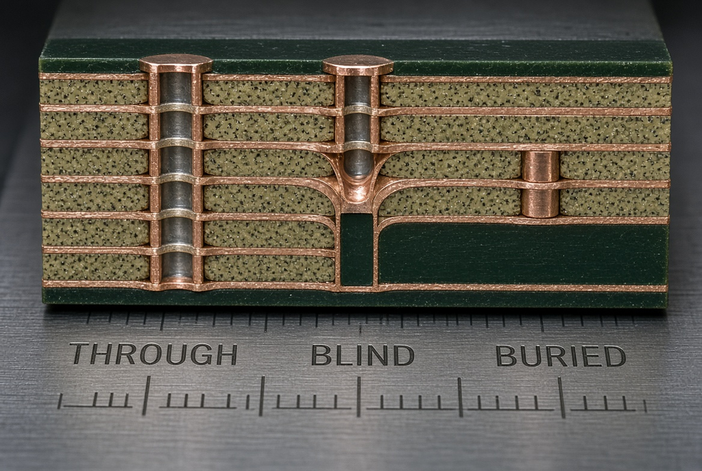
A blind via will extend from an outer copper layer to one or more inner layers and terminate there. It never comes to the other outer face. There’s only one path to go through, that’s why dense layouts take advantage of it: A fine-pitch BGA can route out without punching unused holes in all the other planes and routings layers. Unlike normal vias, blind vias are not an automatic upgrade to an HDI. They require clear layer pairs, typically in sequence, and closer registration. Use them for routing and access, don’t use them as evidence that it is “high density.”
One of the frequent errors is that blind vias are always advantageous to HDI. They address a particular problem of density or the access to layers. They will not fill an existing stack-up with routing channels and they will not obscure a component placement where there was no routing path.
What a Blind Via Actually Is and How It Differs From Through and Buried Vias
A blind via in the fabrication world is a hole that runs from the outside to the inside and has a named layer pair. The CAM file must contain information about the layers that the hole begins on and the layer that it ends on. This pair drives drill method, plating sequence and of course the need for sequential lamination of the board. Without the pair, the shop will have no way of knowing the difference between a blind hole and a through hole that occurs at the same X-Y coordinate.
Blind Via Structure: Outer Layer to Inner Layer Connection
A typical blind via is started on L1 (or the opposite outer layer) and terminates on L2, L3 or a layer in the middle in which the stack-up will actually support it. This outer pad has been plated on the barrel so that it can get to that inner copper. It is the far outer layer that remains while under that location which is the whole point: layers remain unused and do not lose their copper to a through-hole anti-pad.
This structure is only effective if the layer pair is not implicit. A drill file containing holes that have no pair notes makes it impossible for CAM to guess. A 1-2 laser via becomes a mechanical through hole, and a 1-3 pair is referred to as a simple 2-layer drill.
Blind vs Through vs Buried: When Each Makes Sense
Imagine there are two boards with the same BGA pitch. Board A is only allowed to be used through vias. All the escapes steal copper from all the layers they pass, even through planes that do not require a hole. Board B has 1-2 blind vias under the package and maintains the continuity of inner planes wherever a real inner connection is needed. The same density but different routing channels, different layer usage, and typically different process cost.
- Select the type of via from the access problem, rather than from a preference for the vocabulary used for HDI:
- When signals must go both ways, and/or density permits, the default is through vias.
- Blind vias are useful when an outer layer requires a short connection to the first inner layers and the remaining layers should remain closed.
- Buried vias remain within the stack. They help in the inner-layer density but don’t provide an outer pad landing and include their own lamination sequence.
Benefits of Blind Vias in High-Density PCB Designs
Blinds via benefits only appear when routing density or access for layers is an actual constraint. There is a process cost associated with each gain. The board need not be a cleanly routed board with through holes to become a better design by the addition of blind holes. Makes the stack-up more difficult.
Routing Density and Fine-Pitch Component Escape
Blind vias for BGA escape and dense routing work as the via is only present on the layers where it is required. The outer pad may be inserted into the BGA fan-out, the barrel may be plugged into L2 or L3, and the rest of the layers below L2 or L3 landing will remain accessible for planes or other disconnected nets. The via doesn’t free up “more technology.” It releases the routing through-hole channels.
This is a qualitative relationship and must be verified with the actual stack-up and the fabricator’s process:
| Design need | What a blind via can free | What still has to be true |
| Fine-pitch BGA escape | Inner-layer copper under the package that a through via would open with antipads | Layer pair matches the escape layer; pad and capture-pad sizes fit the drill |
| Dense outer routing | Unused lower layers that no longer carry a hole | Adjacent traces and mask dams still meet the finished copper and space |
| Mixed-signal partitioning | A short outer-to-inner path that does not pierce a quiet inner plane | Return path and reference plane are planned in the same stack-up |
| Controlled-impedance escape | A shorter barrel and, in some stacks, a smaller stub than a full through via | Impedance model uses the same reference planes named in the fab note |
Use those rows as guidelines. These factors – pitch, finished copper, die thickness, and drill type – all affect the answer. Avoid copying a neighbor’s 1-2 via into a 1-4 stack and assuming the same escape density.
Inner Layer Preservation and Signal Integrity
The inner layers which are not in the pair retain more continuous copper as the hole stops earlier. It can enhance the integrity of the plane and provide room for inner routing which would be broken up by a through-via field. A blind via can also be used on some high-speed nets to reduce the length of unused barrel as opposed to a through via that extends beyond the target layer.
A signal-integrity gain depends on the stack-up. A 1-2 blind over a poorly placed reference plane will still radiate. It is the return-path via, plane splits and the dielectrics between the signal and its reference that are more important than the word blind. Don’t use the shorter barrel as an alternative to return path design; use it as a tool within a planned stack.
Limitations and Trade-Offs of Blind Vias
Do not use a blind via route if it is still possible to route a simple board. Fabricators do the following sequential evaluations of the feature: stack-up complexity, sequential lamination, inspection access, and cost and yield. They skip the order and the first quote appears to be cheap until CAM opens the files.
Stack-Up Complexity and Sequential Lamination
Named layer pairs are needed for blind vias. Sequential lamination, in which an inner stack is already bonded, and outer layers are added and drilled sequentially, is needed in many constructions, particularly those with HDI blind via applications deeper than the first HDI core. One way to minimize registration risk and late quotes is to add blind vias to a stack that was originally drawn for through vias without re-planning the press sequence.
Laser-drilled 1-2 pairs are not meant to be the same as mechanical 1-3 or 1-4 pairs. Record the pair and the drill plan. There is no such thing as a stack up of “Blind vias somewhere on the top”.
Inspection, Reliability, and Cost Considerations
There are sufficient probes available to probe a through via from both sides. A blind via cannot. Even though electrical test still checks for continuity of net, barrel quality, plating folds and residual dielectrics at target layer are rated through microsection and process control – not by a two-sided visual. This additional inspection process is not a “nice-to-have” report, but an obligation.
Additional registration stack-up, copper plating and another opportunity to register inner voids or misaligned target-pads are added with each sequential cycle. But it’s even harder with heavy copper and large ground pours close to a fine blind via field! These are process effects, not a published, published, copper ceiling.
What Gets Harder as Blind Via Density Increases
The smaller the space, the more soldermask dams and the more tolerance are usually not pleasant as blind via density increases. If a fine pitch is sitting on a large ground pour or a keep out that does not allow capture pads to be placed, a purchasing lead should expect the fabricator to question the fine pitch. Thermal vias on metal-core boards are another heat path: not additional blind vias added on top of an FR-4 HDI structure.
How to Specify Blind Vias So Fabrication Does Not Guess
CAM can construct only things the data names. The package should at least indicate layer pair and via, drill size, and blind or through hole. When the impedance is controlled, the reference planes used for this calculation must be the same as the note. If the product is affected by IPC acceptability class, specify the class. Don’t assume the shop will know what “standard blind via” means for you and select it for you.
Callout Matrix for Blind Via Fabrication Data
Use this matrix on a fabrication drawing or stack up sheet. Implied values in a Gerber file name are not a specification.
| Write this in the fabrication data | Do not leave it implied |
| Layer pair definition (example: L1–L2, L1–L3, L16–L15) | “Blind vias on top” with no start and stop layers |
| Via type: blind, through, or buried, listed separately | One drill file that mixes types without a type column |
| Drill size and finished hole, plus mechanical or laser intent if known | A single finished-hole number applied to every via type |
| Impedance model reference planes that match the pair | An impedance table that assumes through-via reference layers |
| IPC class only if the product requires it | “Standard quality” or “normal HDI” |
| Copper-to-edge, heavy-pour, and dense-via-field notes that affect etch and mask dams | A pretty 3D view with no process note beside the BGA |
Where the Blind Via Note Should Live
Place the controlled note in the stack-up and in the fabrication drawing. This is the document that CAM will construct. A Gerber set containing no layer-pair note, a stack-up PDF containing the note “blind vias on layer 1-2,” and a portal field containing the note “all layers” is three conflicting instructions. Choose one note, say, give it a revision, and alter the revision when the pair changes. If the comment is not a quote-form comment or an email, it would be ineffective unless it goes back to this same drawing.
Cost and Yield Effects of Blind Vias That Do Not Show Up in the CAD Tool
The sequential lamination technique can increase the cost of fabrication, inspection time and risk of failure due to a fine space adjacent to a dense via field. If a fine-pitch BGA is not able to escape from the original through-via stack, the same construction can prevent a board spin. Both those two outcomes are in the same feature. The extra press cycle and microsection sample will not be available on the CAD canvas.
Only compare quotes after starting and finished copper, layer weights, layer pairs and minimum space are equal. If the cheaper number is based on an assumption, such as vias on a file, that this number really requires 1-2 and 1-3 pairs, it is not a savings. It is a “stripped down” version.
Frequently Asked Questions
What is the difference between a blind via and a through via?
A through via runs across the whole thickness of the board and can be accessed from both sides of the board. A blind via is created beginning on the outer layer and ending on a named inner layer. Blind vs through via is a decision of access and antipad: Blind hole does not steal copper on the layers it crosses over; Through hole does.
Are blind vias always more expensive than through vias?
No. They insert process steps if the stack is to be laminated sequentially, plated and inspected for extra purposes. If it’s a board which simply can’t be fine-pitched in any other manner, the additional process is still a cheaper option than a respin. The price is based on the number of pairs and the lamination succession, NOT the word “blind.”
When should I use blind vias instead of buried vias?
Use a blind via from an outer pad to an inner layer when the outer pad is required to reach the inner layer. When the connection is completely within inner layers and the outer surfaces remain closed use a buried via. There is no BGA escape on L1 with buried vias. The inner-only net will not be hidden in blind vias.
Do blind vias require sequential lamination?
Many do, particularly those that extend to the first outer dielectric. Another simple 1-2 laser via can be added after the core, on a thin outer layer. Deeper pairs typically require a predetermined press sequence. It’s the stack-up and not a default HDI label that decides.
How should blind vias be written on a fabrication drawing?
Label the layer pair, record the hole as a blind hole, specify the drill and finished diameters and record it on the stack-up and fabrication drawing. If there is a control on impedance, describe the reference planes for the model. Write the IPC class if applicable. Three conflicting portal fields are one controlled note.
When is an HDI PCB with blind vias the right question, rather than a standard multilayer board?
Request HDI if outer-layer density and/or escape for fine-pitch components cannot be achieved using through vias and a well-thought-out component placement. Once you have opened up through-via holes and cleaned up the board, the simpler question is a standard multilayer stack. If the problem of layer access is truly present, if the pairs are named, and if the fabrication data can be created without guesswork, then blind vias should go into the file.