It’s not a weekend etch job to make a circuit board in a professional setting. A controlled route from a validated schematic to layout, fabrication data, through the manufacture of bare boards, component sourcing, assembly and basic testing. It is not a single lucky prototype that is the objective. The objective is to create a package that can be re-made and will yield the same result.
One of the common pitfalls is to think of copper routing as the entire task. The schematic, stack-up, BOM and assembly data are part of the same workflow as the PCB manufacturing. If one of those pieces is missing or out of revision, the board that is returned will not be the one you thought you sent.
Step 1 — Schematic Design and Early DFM Thinking
The schematic is a electrical contract of the board. It identifies the parts, describes the nets, and indicates the connections that must be made between parts before any copper is drawn. What is not in the schematic is not in the layout. When a net is not found or when a pin is swapped or a footprint does not match the selected package, the defect reaches the assembled unit.
Early DFM thinking should go in this place and not after the first CAM question. The fabricator and assembler are limited by package selection, connector types, test access and high speed topology. Things that seem to be fully designed in the CAD tool may not be able to be built once they are off your desk.
From idea to netlist
The conceptualization of a circuit consists of symbols, values and connectivity. Then Electrical rule checks (ERC) are checked for open pins, conflicting drivers, missing power flag and other drawing errors. Once the sheet is clean, a netlist is generated which will be consumed by the layout editor.
ERC is not just required, but also required. A sheet can pass ERC and still have an old microcontroller, a connector that doesn’t fit in the enclosure, or a footprint that is in the library but not in a distributor’s inventory. The problems will not appear as red markers. They appear later as a “quote delay”, “last minute respin”, or first article that is non-repudiable.
Lock in the manufacturer part numbers that you’re planning to purchase, while the schematics are still cheap to change. If a part is single sourced, or near end of life, make the decision now and add it to the sheet or BOM notes. Allocation of the selected regulator is not a buying surprise, when it’s time to do the kitting.
Design choices that affect fabrication and assembly
There are a few decisions that on the schematic look like they are electrical, but when it comes time to layout become constraints on the manufacturing.
If there is no escape path, then fine-pitch BGAs with no escape path will be forced via-in-pad or extra layers. Fabricator is left with a guess as to the thickness of the dielectrics and weight of the copper on impedance-controlled nets with no stack-up note. Although they may initially connect properly with the board, they eventually fail because they are not mechanically supported and are just soldered on. Test points under a shield or on a 0.4 mm pitch of an unreachable grid make first-article debug slower than it is during the design review, which should have identified and corrected the test points.
Do not put those questions on the schematic as a “fix in layout” note! Write the desired and the reference layer prior to routing if the net requires 90Ω differential impedance. In the event that a programming header needs to remain accessible after the product is boxed, declare that in the sheet that is still the source of reality. Published stack-up, trace, drill and panel data can be used to verify common limits on the fabricator and assembler, rather than having to ask a CAM question.
Step 2 — PCB Layout and Stack-Up Definition
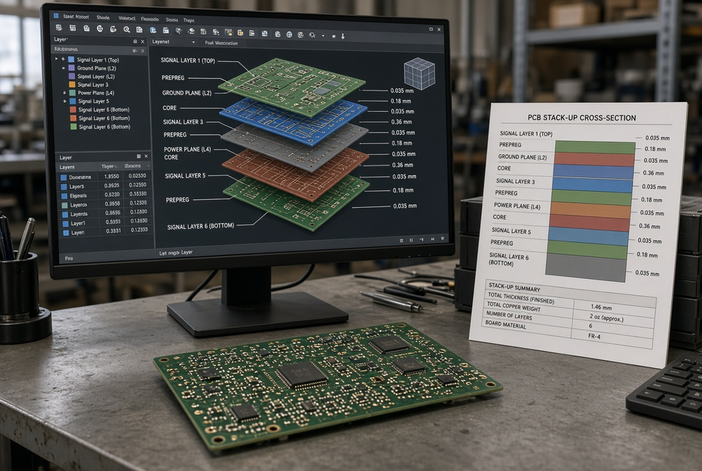
The netlist is placed as copper on the layers in the layout stage. How many of these layers exist, what dielectric is between them, how thick the copper is and whether or not controlled-impedance nets can hit their mark is determined by the stack-up. This stage determines whether or not the board can be manufactured and assembled as planned. It is not simple to make a sloppy stackup on a clean schematic.
Use the stack-up as a manufacturing document, NOT a CAD default. The 4-layer FR-4 category is not a specification.
Layer stack and impedance
A usable stack-up note contains the following information about the layers: layer count, layer order, copper weight per layer, dielectric type and thickness, and any controlled impedances, both pairs and singles, along with their nominal values. If the design contains high speed or RF nets, note should indicate which layers and planes they span.
The typical mistake is to provide the word “4-layer FR-4” to the fabricator, no thickness, no copper weight, no impedance target, and then hope the fabricator would create the designer’s intentions. Multiple default constructions result in different widths of the trace when the same impedance is used. If the edge rate is important on a USB, Ethernet or memory interface, then the stack-up must be written down before the quote is drawn up, not taken from a screen shot.
Prior to imaging, check the stack-up with the fabricator to confirm to the specification. This is less expensive than a respin when the boards are already plated with a short question.
Routing, vias, and assembly access
Routing makes connectivity geometry. Size and placement of trace width, keeping out around connectors all need to endure fabrication and assembly. Vias located under a via-in-pad process note are not solder-void issues. Traces that are near the edge of the board turn into outline and routing risks. Every ground pour that eradicates a test pad makes it more difficult for in circuit or flying-probe access.
Remember to always remember to think about assembly and debugging when routing. Copper that can be reached by a technician or a fixture is required for programming headers, current-sense shunts, and analog test points. If all the firsts are routed to a board and there is no room for a 1.27 mm header, this is not a finished board. It is only routed.
This is the beginning of revision control. The layout revision should be the same as the schematic revision which generated the netlist. The most common way a “finished” design becomes two different products is by updating one file and not the other.
Step 3 — Generating Fabrication and Assembly Data
CAD must create two separate data sets – one for the bare board and one for assembly. They should both be members of the same revision. It is not a complete package to have a Gerber file from Rev B and a BOM from Rev A. It is two half-stories; two different boards.
Name the files, so that it is easy for a CAM engineer and an SMT programmer to know which revision they have without having to open a chat window.
Bare-board data: Gerber, drill, and drawing
Typical packages offered include: Gerber files and/or an ODB++ database, NC drill file, and fabrication drawing. The drawing should include the layer stack, board thickness, copper weight, solder-mask and legend notes, hole attributes, impedance callouts, and any special process notes. Include a dimensioned mechanical drawing if the outline is unusual; otherwise, it is assumed that the contour is defined by the copper edge.
A fabrication package is a layout in PDF or top/bottom copper. This board includes inner layers, soldermask, paste, and legend. So is the drill. If a plated slot, a controlled depth mill or a gold finger is in the design it must be shown in the drawing and not just mentioned verbally in the last design review.
By moving in the form of a structured database, not a pile of files, ODB++ can help minimize the number of mistakes made when mapping layers. Gerber is still in use. When set is complete and units are consistent, and when drawing is congruent with the data, either format is acceptable.
Assembly data: BOM, centroid, and drawings
Typical assembly package includes bill of materials, centroid or pick and place file, assembly drawings, polarity / orientation notes, and test / programming instructions. The BOM is not a distributor SKU, it is an approved manufacturer part number. Write down an alternate if this is possible, with the restrictions of its use.
The two failures keep popping on screen. The first is a BOM that references a number of a catalog item that the assembler cannot purchase to its desired number. The latter is a centroid file that contains designators or rotations that are different from what is found on the board. One stops PCB assembly before the paste reaches the stencil.
The polarity marks on the drawing should agree with the silk and the centroid. A diode, an electrolytic capacitor, a polarized connector or a pin-1 mark that differs across those three files will be manufactured incorrectly by a process that is otherwise controlled.
Step 4 — Bare-Board Fabrication
Once the data is received by the fabricator, the process is CAM Review, material release, imaging, lamination, drilling, plating, soldermask, legend, surface finish, electrical test, and shipment. A smart fabricator will ask questions about gaps prior to lamination. That’s the final, cheap opportunity to correct a missing stack-up note, copper-to-edge violation or an impedance target that can’t be achieved with the selected construction.
When you’re dealing with CAM questions, consider them as a risk reduction. A hold for asking if a pad can be tented is less expensive than a lot of board pads with mask on the solderable surface.
As a Guangdong PCB and PCBA partner, CKS Circuits checks the fabrication and assembly data before production to ensure that the fabrications and assemblies are in step and the files are not allowed to be revised. The review is not a substitute for the designer’s responsibility for the stack-up, drawing and BOM.
What can go wrong in fabrication
The majority of fabrication failures that get to the customer are not found on the plating line, but rather as a result of missing data.
Mask on pads occurs when the soldermask swell is incorrect, or the pad geometry has never been evaluated with the mask layer. Copper within too close to edge of the board is an outline or routing defect. Annular-ring violations include a drill that is no longer located in its pad. If a stack-up is written as a slogan (not a construction) it can’t have a specified impedance, and the fabricator either guesses or aborts the job.
The electrical test ensures continuity and isolation for the bare board from the provided netlist. It does not guarantee that the netlist is the one you intended to publish. If the layout was off of the sheet, the tester would dutifully pass a wrong board.
Step 5 — Component Sourcing and Kitting
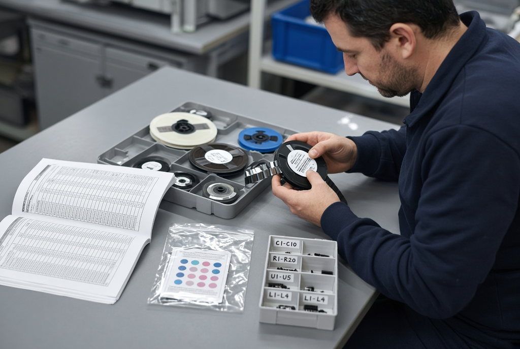
The right parts must be on the line to begin assembly. Sourcing can be turnkey, partial turnkey or consigned. In all models, the objective is the same – trackable and authentic parts (to approved BOM), as needed for the build.
Avoid using kitting as a warehouse task. It’s the final test of whether or not the electrical design is still available for purchase.
Turnkey, partial turnkey, and consigned models
Turnkey is when the partner works under one build package to coordinate the board fabrication, sourcing of parts and assembly. Partial turnkey means the customer provides the partner with some critical parts (typically a programmed MCU, custom connector, or long lead FPGA), and the partner assembles the rest of the product. Consigned is when the customer provides the parts; in many cases, the bare boards, and the partner places and solder(s) the boards, checks them and agrees to the test.
No one of these models does transfer design authority. “Turnkey” does not imply that any substitution may be made without the supplier’s review. A resistor-series change, a regulator second-source, or a connector family change are not items of a packing list, but are part of a written approval.
Model ownership of risk is not judged by the completeness of word sounds. If a customer has programmed devices, then the devices are consigned. Customers who require one workflow for a typical BOM can apply turnkey. When the two mix without revealing who bought what there’s a shortfall in the kits.
Availability, alternates, and lifecycle
Availability, life status and approved alternates must be checked prior to the build, not after the stencil has been cut. Even if a BOM will work nicely in the CAD library, it may not be possible to purchase it in the necessary quantity for the desired window. That includes last time buy notices, packaging issues (reel versus tube), moisture sensitivity differences between an approved part and a “close” alternate, etc.
If the project needs help buying and coordinating parts as part of a turnkey or partial-turnkey build, component sourcing for PCBA is the point in the workflow where BOM risk, alternates, and kit completeness should be closed. Do not leave an empty manufacturer column and assume the line will invent an approved source.
Step 6 — PCB Assembly and Basic Test
The assembly process consists of: Solder Paste Printing, Component Placement, Reflow or Wave Soldering based on the technology mix, Inspection and The test the project actually agreed to conduct. The result is a PCBA, that is a board with the same joints, polarity and firmware as the design package. Parts that are in pads are not parts that are sitting on pads.
All these must correspond to the package mix on the board. A design that combines a large electrolytic, a fine pitch BGA and a row of 0402 passives requires a profile, and a support plan is required that will serve all three, not just the one the programmer was concerned about.
Inspection and first-article validation
Some of the common in-process and outgoing checks are solder-paste inspection (SPI), automated optical inspection (AOI), X-ray for BGA and other hidden joints, and first-article inspection against assembly drawing and BOM. The checks vary based on package mix, order and quality plan. They are industry standard, not the assurance that every factory uses every method each and every time.
The first article should not be just ‘checked’ but tested against the design intent. Those are in that check, like power rails, programming, smoke-free boot, and the interfaces that the product uses. If a first article is approved using a development firmware image or a hand-fitted replacement or another BOM revision than what would be used to make the product, then it is an unrepeatable process.
Document the configuration: Board revision, BOM revision, firmware hash, test fixture and any rework. If this record does not exist, then the next lot will be an experiment that is new.
From first article to repeat builds
There is proof that one unit can be constructed from a first working board. For repeat production, the same stack-up, approved parts, stencil and profile notes, and test limits must be used. The decision to change a decoupling capacitor “because stock was short”, to thicken the copper “because the last lot felt thin”, or to pass on a functional test because an AOI looked clean” makes a second product with the name of the first product.
Revision control is the distinction between prototype and process. If the schematic, layout, BOM or test instruction change, the revision will change. The next purchase order should reference that revision, NOT a conversation from the first build.
Common Mistakes in the End-to-End Flow
The majority of these failures aren’t “mysterious”. These are mismatches that became apparent before they had ordered for laminate.
Schematic and layout drift
If the schematic is updated and not the layout (or vice versa), the nets, footprints, and board will be mismatched with the BOM. ERC and DRC will have a problem catching a designer who published two separate revisions under the same project name. Prior to exporting Gerbers, be sure that the netlist in layout was generated from the sheet you will be saving.
The cost is displayed as a mis-stuffed wrong value, a missing pull-up, or a connector pin-out does not exist on the old sheet. None of these is a fabrication defect.
Fabrication data without stack-up or finish
A Gerber set that has no stack-up or copper weight or surface-finish note means the fabricator has to make an educated guess. This quote then begins to make assumptions. Boards may fail a simple continuity test and still be electrically incorrect if the assumptions are different from those you made in the impedance model you used for the layout.
Add construction to the fabrication drawing. If it is important they have finished their reading, the notes are not what you are looking for.
Assembly data without alternates or polarity
If no alternates are approved for a BOM, the BOM will stop when the main part is short. The boards look crowded and don’t function if the centroid has no polarity or it is against the silk. Both problems are easier to correct in the package of data than on a populated panel.
If there is no second source, state this. A single source risk, with documentation, is usable. An empty alternate column does not qualify as a risk register.
A Simple Workflow Checklist for How to Make a Circuit Board
Have these answers in mind before you ask for a quote. If one of the lines is a no, the package is not ready.
- Is the schematic stable, revision controlled and ERC clean?
- Are all BOM numbers on the sheet equal to the BOM you will send?
- Are there any targets for the stack-up (copper weight, direction of the dielectrics, etc.)?
- Do the Gerber / ODB++ files, the drill file and the fabrication drawing represent the same revision?
- Are finish, mask, legend, outline and special processes given explicitly rather than left to reader’s understanding?
- Does the BOM contain approved manufacturer parts and alternates (if any) written by the design team?
- Are there consistencies between the centroid file, assembly drawings and polarity marks?
- Do test, program and first-article expectations exist and are these documented along with the firmware and fixtures to be used?
- Are schematic, layout, fabrication data and assembly data all the same revision letter?
The actual result of this workflow is a full response to that list. The boards after it can be rebuilt. The boards which skip it could be made just once, and no one will ever be able to explain why the second lot is different.