What Is a PCB? Printed Circuit Board Structure, Functions, and Uses
A printed circuit board is a sheet of fabricated dielectric material with copper conductors, pads and vias that mechanically hold electronic parts and electrically join them together. If you’re wondering what a PCB is, the first thing you should think of isn’t the componentry on it, but rather the board itself. The board is built without components and leaves the shop unassembled.Board is assembled empty from the fabrication shop. Those parts are then mounted and soldered to create a PCBA, which is then inspected to ensure the build is correct.
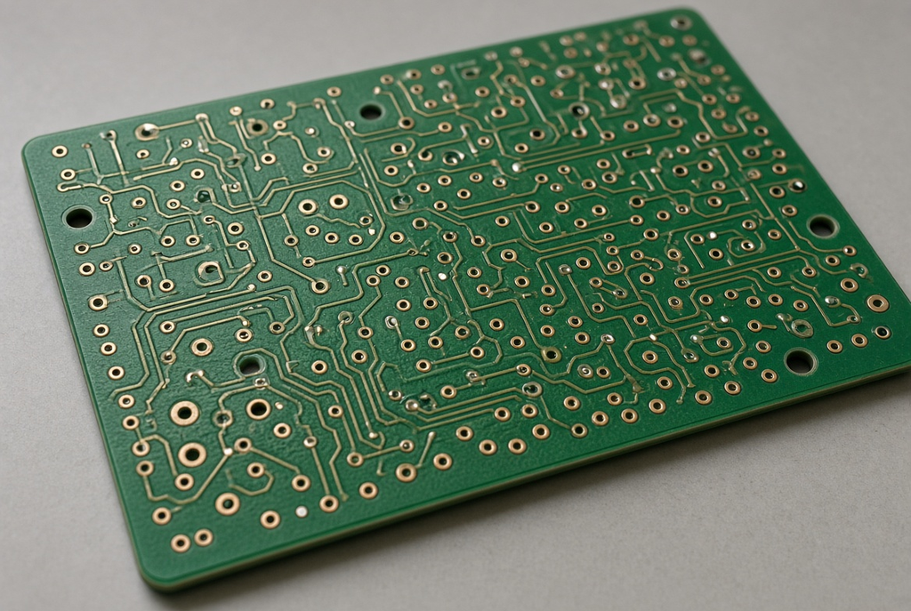
This article will discuss the structure of the printed circuit board, the function of the board in a product, common applications of the board, and the information a factory must have before they can manufacture it. A picture of a controller populated with green do not indicate a Green product. This picture does not indicate the number of layers, copper thickness, surface quality or if you are only needing to be fabricated.
Separate the Schematic, the Bare PCB, and the Assembled Board
Electrical idea is the schematic. nets, parts and how they communicate. The PCB is the actual board that contains the interconnects and the mechanical base is the board on which the PCB sits. Once the parts are soldered on and the assembly is tested as per the agreement, it is the same board that is known as the PCBA. Those three objects get mixed in when purchasing weekly and it generally begins with a picture.
A person on the buying end takes a picture of a working controller and requests “the same PCB.” The image depicts a scene with several items, including people sitting in front of a green mask and some logos. It does not indicate the number of copper layers within the laminate, copper weight etched, surface finish of the pads or if the previous order was just fabrication. You’re going to have to come up with a stack-up when you quote that photo as a bare board. By citing as an assembly without a BOM and centroid file, it creates the parts list. Both quotes don’t match the product on the bench.
What a blank or bare board includes
A PCB that is empty, without parts or without components is still a finished fabrication job. It already has laminate, a copper pattern, copper holes in the laminate, legend, a surface finish on the exposed copper and, typically, an electrical test of the nets. The term “blank” is not synonymous with unfinished, unmasked, or unfinished product. Also, it’s not a perfboard. Copper is already provided for a design.
You get the bare board when you purchase only the fabrication – treat it as such. If the team requires that board to be fabricated from Gerber data and a fabrication drawing they can ship the package for PCB fabrication. The word “working boards” on the purchase order does not match with the word “bare panels” on the quote.
Treat the bare board as the deliverable you receive when you buy fabrication only. Teams that need that board built from Gerber data and a fabrication drawing can send the package for PCB fabrication. If the purchase order later says “working boards” and the quote was for bare panels, the two sides are not talking about the same object.
How a Printed Circuit Board Is Built Up
Read the board from left to right and from top to bottom, just like reading a cross-section. All the layers that can be named are part of the fabricated board. Each note without a factory, is a guess that the traveler has to make.
Laminate, copper, solder mask, and legend
The usual starting point for the rigid boards is FR-4 glass-epoxy. This is not the only material. The laminate is the material that contains copper, determines thickness, and brings thermal and mechanical properties of the finished panel. Name the material as family on the drawing. NEVER assume from a picture of a green board that its owner has left the shop.
The weight of copper is related to the amount of current a conductor can transmit, and to the etching of the image. Different etch allowances are required for a heavy vs. light signal layer. If the drawing indicates one weight, but the drawing appears to be another, STOP and clear the note before imaging the panel.
Solder mask should be used to cover copper to which you do not want solder to be applied and open pads that need soldering. Common green is not because the circuit needs to be green, but because the imaging process is mature. The colour of the mask is a process decision. It is NOT a substitute for a fabrication note on clearance, dam width or which copper to keep open.
Legend (or silkscreen) provides assembly information: reference designator, polarity marks and version text. Not related to electricity. There is no stack-up, finish or copper weight indicated on a mask. If the cosmetic treatment on artwork is considered the manufacturing specification, then the panel is built to the wrong drawing.
Traces, pads, planes, and vias
Traces are the conductors that are routed to provide connections between lands that carry signals and power. Lands parts or contacts that use pads. Planes are wide pieces of copper for power or return. Vias are the places where the connections between the layers are plated. Blind and buried vias are denser hole structures which do not extend through the entire stack; these should be referenced in the fabrication note for the design rather than as a general term for any multilayer boards.
The artwork may have Copper that appears open but is actually covered by mask. Depending on the fabrication note, a via can either be tented, plugged or left open. The note will otherwise be missing and the shop will select a default which may be incompatible with the test probe or may leave a hole you expected to be closed.
Structural elements and what is required in fabrication of PCBs.
PCB structural elements and what fabrication needs
| Element | What it does | What must be specified |
| Laminate | Dielectric core that supports copper and sets board thickness and thermal behavior | Material family, thickness, and any special thermal or electrical note |
| Copper | Conductive foil that becomes traces, pads, and planes | Copper weight per layer and which layers carry that weight |
| Trace and space | Routed conductors and the gaps between them | Intended minimums on the drawing so etch and registration can be checked against the artwork |
| Pad | Land used by a part, connector, or test point | Size, shape, and whether the pad must stay free of mask |
| Via | Plated hole that connects copper layers | Drill size, start and stop layers, and whether the hole is tented, plugged, or open |
| Plane | Broad copper for power or return | Which layers carry planes and any keep-out or split-plane note |
| Solder mask | Insulates copper and opens solderable lands | Color if it matters to the product, and which openings are required |
| Surface finish | Protects exposed copper and affects solderability | Finish type on the drawing; do not leave exposed copper unnamed |
| Legend | Assembly markings on the board surface | Color and which text must remain readable after finish |
A surface finish is applied to bare copper and can have a significant influence on the characteristics of the soldering joint. Label the finish on the Fabrication Drawing. Avoid using “HASL or whatever you use” as a specification.
Single-Sided, Double-Sided, and Multilayer Construction
There is a reason for extra copper layers: more routing, a power/ground plane, controlled impedance, or a denser parts. Sometimes a 2-layer board is the correct board. In the last project, you used 6 layers, you could reduce the number of layers if you were to call it “multilayer” without defining the stack-up, as you are still consuming lamination that you could be using for the other layers.
A single-sided board is the one that is copper on one side. A double-sided board with copper on both sides and holes that should be connected with nets on both sides of the board. A multilayer printed circuit board includes inner copper layers that are added to the dielectric material. That step includes registration, a list of PCB layers and stack-up and a drawing that specifies layer count, dielectric, and copper weight. Any request for “multilayer” without a number of layers, a dielectric, copper weight and/or impedance note is not a buildable request.
Multilayer PCB construction is what you are specifying when you use a laminated stack-up with the design instead of just 2 copper layers. The stack-up must go along with the Gerbers. The order of the layers cannot be restored from a photograph of the top of the stack.
Other constructions, stated only as a boundary
There are other families of flex, rigid-flex and HDI. When the product requires to bend, changes from a stiff area to a flexible area or density via microvias, they are created. They are not the subject of a type-selection exercise in this article, and they are not automatically an alternative to a non-flexible stack-up. If the product requires one of those constructions, name it on the drawing and send them the stack-up belonging to it.
What the Board Does in a Product
The board performs three tasks, none of them is abstract circuit theory.
It establishes the desired connections and sometimes it serves as a return path. Traces and planes are that job. The schematic promise does not appear in the product if the net is not present in copper.
It can be used to locate parts in a repeatable location for assembly and for the enclosure. Pads, holes and outline dimensions are that job! If the board fits into the fixture but doesn’t have the mounting holes, it is the wrong board.
Can distribute heat and offer mounting points. That help is actual on an LED area or a power area where there is a need for additional copper or a material path that is different from a low-power logic area. Not a full design (thermal or mechanical). The remainder of the heat in the copper must be removed through a plane, a metal-core path, a heat sink or through the enclosure. It’s a standard FR-4 signal board, and is not to be used as a thermal solution, as it has a few wide traces.

Function starts after assembly
The three jobs come up only after the correct parts are soldered and as agreed the assembly is checked. If the buyer required a working assembly, then a bare board that passed the electrical test—opens and shorts in the fabricated nets—could very well be the wrong deliverable. Bare PCB is NOT a quality issue, it is a purchasing decision, and it is one that hinges on the quality of the same product.
If the deliverable is populated board, this is PCB assembly and will be accomplished by the SMT or through-hole method as part of the assembly process. For Fabrication, it’s the interconnect that is fabricated. The parts are assembled using assembly. The most frequent hand-off mistake between the hardware team and the shop is ordering one when you really wanted the other.
Where PCBs Are Used, Without an Application Tour
The printed circuit board (PCB) is present in nearly all electronics. The helpful question is not the marketplace label. It’s what the product is asking the board to do.
Stable mounting, clear connectors and sufficient copper for mixed signal/power on the same panel are often required in industrial controls. Consumer devices typically sacrifice outline, thickness and number of layers for a small enclosure. Compact stack up and clean antenna or interconnect region may be necessary for connected sensors. Impedance notes and a documented stack-up become a necessary part of networking hardware. Lighting, particularly LED areas, relies on copper and thermal path more heavily than additional layers of signals. Test equipment sometimes requires a hard outline, easily accessible test points and a finish that will withstand repeated probing.
Industry fit is dependent on the project; and on proven manufacturing experience. Never make a statement of capability with a sector name, and don’t jump to the conclusion that the same stack-up goes from a logic board to a high-current lighting board.
What a Factory Needs Before It Can Build the Board
A manufacturer cannot determine the board from a schematic display. It is not the picture of a working product that a PCB manufacturer requires, it is a package of fabrication.
Typically this consists of a Gerber or ODB++, a drill file, and a fabrication drawing. For that drawing, enter the number of layers, the finished thickness, the weight of the copper, the material, the surface finish, the mask and legend, and if the design is provided, enter the impedance notes, if any, or the panel notes, if the buyer already has the array. Those PCB fabrication files are the ones that are used to image the copper, drill the holes and laminate the stack at the shop. A lack of one doesn’t make the others more informative.
A pre-production review is used to detect conflicts as files are still in the state where they can be changed: mask covering a pad that is designed to solder, copper too near to the edge of a board, a stackup that fails to meet a specified impedance, or a drill that leaves no annular ring. In production, CKS Circuits, Guangdong PCB and PCBA manufacturing company, checks the fabrication data and asks these questions before producing the panel.
Engineers preparing stack-up, trace, drill, and panel data can use PCB design guidelines as a next check before the package goes out.
The incomplete-file pitfall
Only the top copper art, a layout PDF or a logo file will cause the quote to collapse. It then becomes a guess what is the number of layers. Finish becomes an automatic houseplant. If a last similar job was done, then the thickness will become what was used in that job. A board which does not match the picture can be delivered and still be the product.
Indicate decision and engineering review items. If the weight of the copper is not changed but the impedance is, indicate as such. Say if the outline is locked, but the stack-up is not. Lack of comment on those matters does not constitute flexibility. It is a challenge to make two boards with the shop and the buyer.
What Is a PCB: What to Remember Before You Order
The fabricated board of copper and dielectrics is called PCB. Printed circuit board structure must be indicated: laminate, copper, holes, mask, finish and legend. The product function is seen after the product is assembled. An usable order is not just a picture or schematic, but it contains fabrication data. If the four sentences above match the files on your desk, you are speaking about a board that a factory can construct.