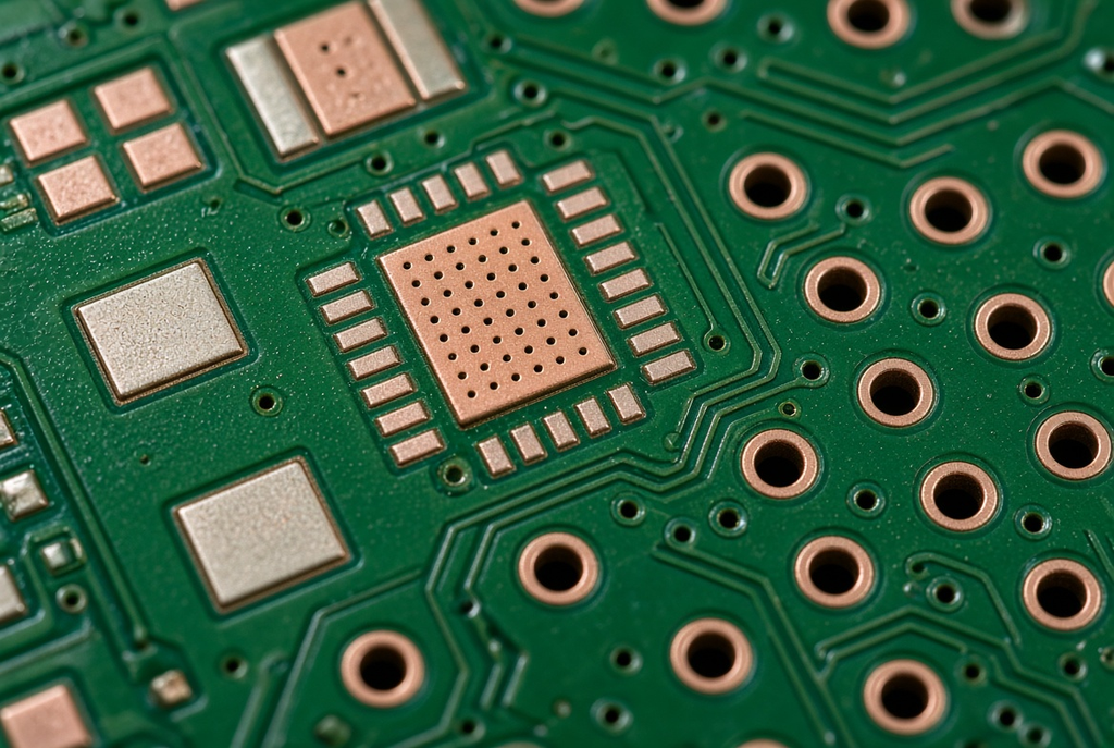
PCB Pads: These refer to the copper pads on the board that are used to make the connection with the component. They aren’t only shapes that “fit” a footprint. Whether it wets, remains aligned and passes inspection depends on the geometry of the pad, the solder mask opening, surface finish and solder paste volume. Consider pad design as a package-plus-process decision, and you won’t have the typical assembly issues: starved joints, tombstoning, bridging, and parts not seated on the pad.
It’s the misconception that any pad size will do so long as the part lands on copper that CAM and SMT teams most commonly encounter. A 0402 resistor requires a different set of pad geometry guidelines, mask definition and the paste rules are different as well.A 0402 resistor requires a different set of pad geometry guidelines, mask definition and the rules for pasting are different also. Match the pad with the package, assembly and the finish of the copper.
What PCB Pads Actually Are and How They Function
A pad is a defined copper feature that has a mask opening, finish and has a role in the netlist on a fabrication drawing. The volume is the part in the stencil and the line that holds the solder for self alignment. Both of these views need to be in agreement. In some cases the CAD library pad may not conform to the manufacturer’s recommended land pattern or the mask opening may not be drawn with the solder mask defined versus non-solder mask defined pad and the board may still etch correctly, but fail despite reflow.
Pad Functions: Electrical Connection, Mechanical Support, and Thermal Dissipation
The obvious one is electrical connection. The “pad” is the area between the terminal for the component and the trace/plane. Even if the copper is small, the joint may appear to be wetted, but may still cause the current path to be starved or to create a high resistance interface after thermal cycling.
It’s easy to underspecify mechanical support. The part is placed on the molten solder during reflow. During cool down, the fillet is what holds a chip resistor in place and is what provides a little bit of pull-out resistance to a connector. SMT pads are based on the area of land and the fillet shape, while through-hole pads include a barrel copper and an annular ring. Tombstoning and poor heel fillets between pads are apparent on the AOI when the pad is designed as an electrical node, not considering fillet length and/or pad-to-pad balance.
Thermal dissipation is the heat path into copper and possibly into a via if necessary using the pad. A large thermal pad and a non-flooding paste pattern is typically required for power packages and QFN slugs. The problem is to take a full pour of copper under a slug and then open 100% paste and wonder why the part is floating or voiding.
SMT Pads vs Through-Hole Pads: Different Requirements
Imagine two boards using the same “family” of connectors. One is an SMT footprint (rectangular lands, no drilled barrel, solder volume set via the stencil). The other uses require the use of thru-hole pads: barrel filled with plated holes, annuular rings, and a wave, selective, or hand solder connection. Same schematic symbol. Various land, various solder joint, various inspection standards.
Select the type of pad and the line used to create the board from the library footprint in the actual package, rather than the library footprint of another package. For mixed-technology boards both styles must be used on a single board. That is normal. What’s not normal is when someone copies an SMT land under a through-hole pin, or has a through-hole pad on a heavy plane and expects hand soldering to heat the joint in a reasonable amount of time.
Solder Pad Design Principles for Reliable Assembly
Solder pad design is a set of rules, and not a one-size-fits-all rule for all packages. Land Size is correlated with the Mask Opening, Finish and Paste Aperture. Always consult with the component manufacturer to see if the component can fit the land, and then verify the mask and copper features you are designing can be held by the fabricator. Please do not use any of the numbers found in this section as a process limit for a given shop.
Solder Mask Defined vs Non-Solder Mask Defined Pads
Solder mask defined (SMD) pads have a mask opening less than the copper so the mask defines the land, and the copper is set by the mask opening. The non-solder mask defined (NSMD) pads ensure that the copper size is smaller than the mask opening, therefore the copper edge is free and the solder can wet the pad sidewall.
| Topic | Solder mask defined (SMD) | Non-solder mask defined (NSMD) |
| What sets the solderable area | Mask opening | Copper pad size |
| Mask relationship | Mask overlaps copper | Mask clears copper |
| Typical preference | Fine-pitch lands where a mask frame helps contain solder and stabilize pad size | Many BGA and discrete lands where sidewall wetting and a defined copper edge help the joint |
| Watch-outs | Tight mask registration; dam width between openings | Copper-to-copper spacing and mask sliver between openings |
| How to treat the values | Guidelines only; confirm mask expansion and registration with the fabricator | Guidelines only; confirm copper size and mask clearance with the fabricator |
There is no “better” or “worse” aspect to either style. This can be a mask defined hole in fine-pitch QFN or some CSP lands that keeps the solderable area uniform even if the copper is etched too big or too small. NSMD is preferred by many BGA balls because the ball will wet the edge of the pad. Write the selection in the fabrication notes. You can leave it implied or leave it unmarked and discover it when the first article is X-rayed and you see it’s NSMD.
Pad Size and Geometry for Different Component Packages
PCB pad sizes are NOT listed by individual house number, but by package. A 0402 chip resistor requires short, well balanced lands in order to equalize thermal mass on both ends. 0603 and 0805 provide a greater fillet room, but the same balance rule is followed. SOP and SOIC lands are longer and typically have a toe/heel portion to allow the gull-wing lead to create a visible fillet.
QFN and LGA packages include a center thermal pad and perimeter signal pads. Perimeter lands are typically narrower than may seem casual from a library and crowding can result in solder bridging. BGA pads are round and are sized in accordance to the diameter of the ball used, the size of the pad is driven by the pitch. A 0.8 mm pitch BGA land is a common library error when copying onto a part with a 0.4 mm pitch.
Start by using the land pattern recommended by the component manufacturer, then add your house rules for mask and paste. Avoid creating a second library simply because it “looks close. If there are two identical elements in CAD that don’t have a footprint on the data sheet, divide up the footprints before you send out Gerbers.
Surface Finish and Solderability Considerations
It is not the copper pad that the solder experiences first. The finish of the surface is. HASL leaves a solderable tin-lead or lead-free coating which is well known on coarser pitches but may be irregular on fine lands. ENIG provides a plane surface of nickel-gold coating, which contributes to the planarity of fine pitch and BGA. OSP is a thin organic layer that forms on copper, and it will solder to copper if the shelf life and/or number of heat cycles remain within the working range of the finish.
Complete choice changes; wetting speed; board can sit before assembly; number of reflow cycles that the pad will endure. It is not an alternative to the pad geometry. A land on OSP that is starved will continue to be starved. Use the same finish (or assign a finish) on the fabricating drawing and on the assembly quotes. The switch to ENIG and the change of yield between prototype and production can be made in a quiet manner, by simply changing the paste and profile notes between the two.
Via-in-Pad and Special Pad Considerations
A special pad is not for decoration of a dense layout but to solve a routing or thermal problem. Take a walk on the decision path as a fabricator does: is it necessary to have the density, is the pad still solderable, must the via be filled and capped, what will happen to solder during reflow. It is not necessary to use via-in-Pad on every Fine Pitch part.
Via-in-Pad Design and Assembly Implications
When using a via-in-pad pad, a via is placed in the land so that a trace can drop directly below a BGA, QFN or other tight package. This leaves escape routing free. It also provides a route for solder to wick into the via if it is not completely filled.
For via-in-pad, indicate treatment such as tented, plugged or filled and if the pad needs to be capped and plated flat. Open via in BGA pad will take the solder material from the solder ball. An un-levelled cap may tilt a QFN. The design note should be included in the fabrication data, not in a subsequent e-mail when the initial panel returns with X-ray voids.
Thermal Pads and Heat Dissipation
Thermal pads are located under power packages, LED emitters and QFN slugs on PCB layouts. They distribute heat to copper and, if available, to a via stack up and/or to a via metal core path. The heat paths are not additional pad types. They are identical copper land for thermal jobs.
The design is as important as copper area. If the part is a large slug, a good, clean 100% paste print will generally result in the void or float of the print. Typical production method is a windowed or hatched stencil opening in a stencil that conforms to the via pattern. It is important that thermal vias located in a slug pad be treated similarly to other via-in-pad features; otherwise, solder will drop in and fill the vias.
Test Points and Probe Pads
Test points and probe pads must be sized and accurately finished in order to be probed by the flying probe or fixture, and be of a known size to ensure reliability of contact. The fabricator or assembly house will want to know if the pads are for trouble shooting, flying probe or bed-of-nails for a purchasing lead. “Add test points” (no diameter or finish note) is not a full requirement.
Common Pad Design Mistakes and How to Avoid Them
The errors that make it to CAM are redundant. Lands that have been taken from an old library are too short for the current package. The definition of mask remains as the default setting of CAD. With a plane-connected-through hole pad, the soldering iron will not be able to heat the barrel because there is no thermal relief. Different pad geometries are used for two connectors in the same family on the same board. The notes in the assembly file indicate “fine-pitch” and the Gerbers indicate standard chip lands.
If a stated workmanship class has been required for the product, indicate the class on the drawing. The word “standard pad design” is ambiguous to the fabricator. If impedance is controlled elsewhere on the board, ensure that it remains the same across the pad and anti pad.
Callout Matrix for Pad Design Fabrication Data
| Write this in the fabrication data | Do not leave it implied |
| Pad geometry and size for each land type (chip, SOP, QFN, BGA, through-hole) | “Use standard footprints” or a CAD library name with no dimensions |
| Solder mask definition: SMD or NSMD, plus mask expansion or clearance | Whatever the default mask swell happens to be in CAM |
| Surface finish on the pads | “Any solderable finish” |
| Via-in-pad requirements: fill type, cap, and planarity if the via sits in a land | An unmarked via in a BGA or QFN pad |
| Thermal relief on plane-connected through-hole pads | A solid plane tie with no spoke note |
| IPC workmanship class only if the product actually requires it | “Standard quality” or “IPC pads” with no class |
| Assembly notes: paste considerations, thermal-pad stencil intent, mixed SMT and through-hole process | A portal field that only says “fine-pitch assembly” |
Where the Pad Design Note Should Live
Put the controlling pad note on the fabrication drawing and the assembly drawing. Maintain one statement per revision. No pad note, a stack-up pdf that states “standard pads”, and a quote form that states “fine-pitch assembly” are three documents stating three different things.
Update the drawing if the land pattern or the mask definition is changed. Never add the change to an email thread and not delete the old note from the file. Follow files will be followed by incoming CAM.
Cost and Yield Effects of Pad Design That Do Not Show Up in the CAD Tool
Plus, process steps, like via-in-pad, filled/capped vias, extra-flat finishes and dense mask-defined lands. Those steps can increase the fabrication cost and may introduce assembly time, when the paste and planarity need to be qualified. Also, they can help avoid a board spin if the first layout left insufficient amount of copper for a good joint.
Cost which is not reflected in the autorouter is scrap from the following: (a) bridging on narrow QFN lands, (b) tombstoning on unbalanced chip pad, (c) wicking of solder into open vias, (d) parts which fail the X-ray due to the thermal slug voiding. Compare quotes only when pad geometry, mask definition, surface finish and assembly notes are all the same on all packages. A lower cost board, different finish or an open via-in-pad is not a different board.
Frequently Asked Questions
What is the difference between solder mask defined and non-solder mask defined pads?
Solder mask defined pads have the mask opening smaller than the copper, the opening is the solderable area. For non-solder mask defined pads, the copper area is smaller than the “opening” of the mask, so the edge of the copper is exposed and will allow solder to wet the side wall. Select the style from the package and the assembly process, and label it on the fabrication drawing. Overlap and clearance values are only guidelines and should be checked for capability.
How do I choose the right pad size for my component package?
Begin on a land pattern suggested by the component manufacturer. Only change settings for mask definition, pasted aperture, and house rules that have been documented. Balanced lands are required for chip parts. Parts of the QFN and LGA type require a perimeter lands and designed thermal pad. BGA pads are ball-to-pitch size. Avoid using the same footprint that was used next door, since it is not exactly the same.
Are via-in-pad designs always required for fine-pitch BGAs?
No. via-in pad is the answer to escape routing while in a close package. It is possible to route out either on the surface or on the following layer without making a via in the land so it is possible to forgo the fill-and-cap step in many cases. If it is necessary to use via-in-pad, the following parameters in the form of constraints should be set to prevent solder wicking into the hole: fill-planarity, cap-planarity and pad-planarity.
What surface finish is best for solder pad reliability?
No one finish is best. When the pad geometry is correct, the pad finish is within its working window, and the soldering conditions are suitable, then HASL, ENIG and OSP can all be soldered. ENIG tends to be selected for flat fine pitch lands. HASL is very common on coarser features. OSP requires more management over storage and heat cycles. Compare builds by calling out the finish.
How should pad design be written on fabrication and assembly drawings?
Include State pad geometry, SMD or NSMD, surface finish, via-in-pad treatment, thermal relief and any required workmanship class in one controlled note on the drawings. Avoid breaking the requirement into a Gerber readme, a stack-up pdf file and a quote form.
When are special pad designs justified instead of standard pads?
Density, heat and package geometry routing actually needs use via-in-pad, large thermal slugs or unusual mask definition. If a standard land in the component data sheet will assemble cleanly, retain the standard land. Extra process features should be added to a real routing or thermal issue, rather than to a preference in the CAD library.