
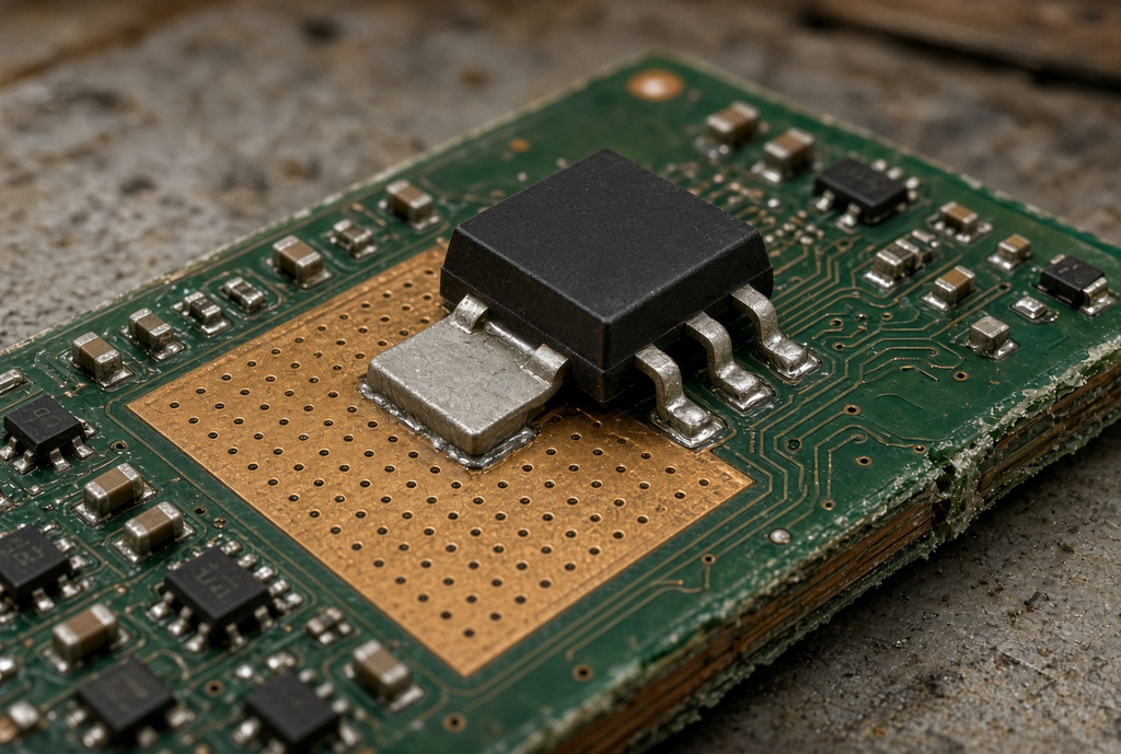
Thermal Vias in PCB Design: Sizing, Placement, and Heat Dissipation
This guide is for PCB designers, hardware engineers, and thermal engineers who treat thermal vias as a heat path, not extra holes. It explains how via size, count, placement, fill, and thermal pad design change component temperature, and how to write those choices so fabrication does not guess.
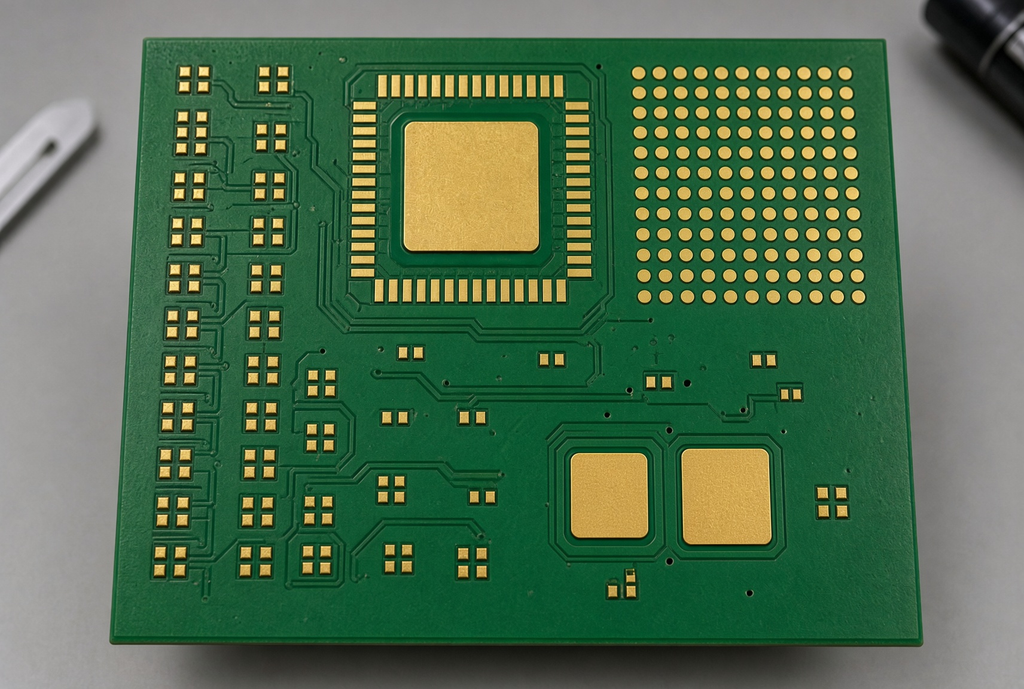
PCB Pads Explained: Types, Solder Pad Design, Sizes, and Common Mistakes
A practical guide for PCB designers, hardware engineers, and layout engineers who need clear pad decisions. It explains pad types, solder pad design, PCB pad sizes, mask definition, via-in-pad and thermal lands, and the fabrication notes that keep assembly yield from collapsing on first article.
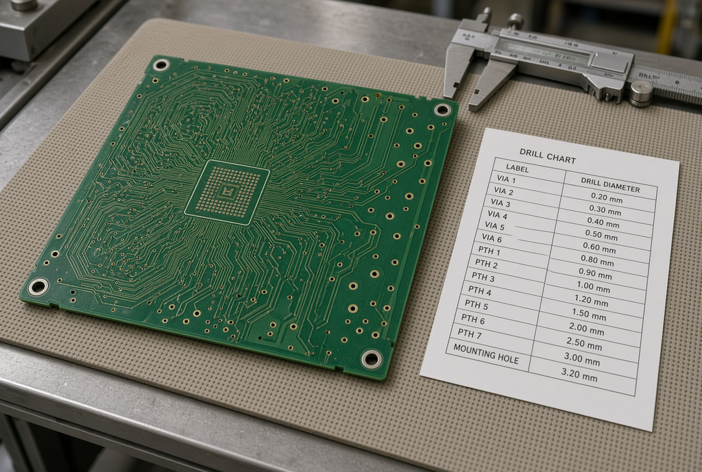
Standard PCB Via Sizes and Drill Sizes: A Practical Design Guide
This guide is for PCB designers, hardware engineers, and layout engineers who need to specify via and drill sizes without guessing. It explains how drill size, finished hole size, annular ring, and aspect ratio affect routing density, fabrication yield, and reliability, then shows how to write those values so CAM does not infer them from a CAD default.
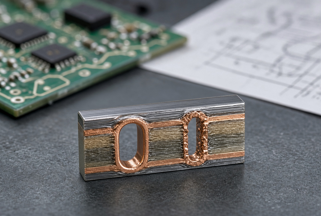
PCB Via Plating Thickness: Requirements, Reliability, and Manufacturing Control
This guide is for PCB designers, hardware engineers, and quality engineers who need to specify via plating thickness instead of leaving barrel copper to a factory default. It separates via barrel plating from surface copper, explains how reliability, current, and aspect ratio change the requirement, and shows how to write fabrication notes and inspection methods so plating thickness is controlled rather than assumed.