Via-in-pad is a via located within a component pad to allow for traces to go under a fine pitch BGA, QFN or LGA without having to use the entire first routing ring for dog-bone fan-out. That move opens channels, and shortens the first hop off the package. It also alters the pad design, pad-in-pad filling, plating, capping and solder-paste work. Use via-in-pad to solve density issues, don’t use it for all BGAs. If solder is to be wicked into an unfilled hole in a small pad, or if the fill in a board is too large to be fanned out then there are process steps to be added that are not necessary.
It is generally believed that via-in-pad will always be preferable for BGA. It is not. It is used to solve escape and density where traditional fan-out will not fit. It’s not a replacement for package placement, stack-up planning, or a cap which can still create a good joint after fill and cap.
What Via-in-Pad Actually Is and How It Differs From Traditional Via Placement
Via-in-pad is a location rule + construction note in the fabrications language. It is not located next to the land, but within its boundaries. The drawing must then specify if that barrel is open or closed, filled or not filled, capped or not capped, so that the pad remains planar for paste and pad placement. The four options—location, fill, plating, and cap—determine what you’ll get on the solder, and how the assembler will behave in reflow. The wicking and starved joints appear on first article when they are copied from a standard SMT pad with no notes on the pad.
The typical production solution for a level land is to use the construction via construction (via-in-pad plated over) technique, which involves filling the barrel, then plating a layer of copper over the fill and, finally, presenting a capped surface that can accept paste. The acronym comes in handy on a drawing. Is not a stand-alone specification.
Via-in-Pad Structure: Via Located Directly in Component Pad
The via drill, plating barrel and the pad copper are all of the same size. On a fine-pitch BGA, this frequently means the via is either in the center of the ball land, or slightly inboard, covered and capped so the assembler doesn’t see a hole in the pad. The final land remains the same as the package footprint, it is still part of the pad; a via is not a bonus feature that you can do without because it has become part of the package footprint.
The problem is to use the same pad geometry for the same pad geometry as a solid land next to a traditional via. Capillary path is an open barrel under a small ball or QFN thermal pad. When the solder is reflowed, it takes that route into the hole. The deposit of the stencil may appear to be correct on the printer and the joint on the land may still become lean.
Via-in-Pad vs Traditional Via Fan-Out: When Each Makes Sense
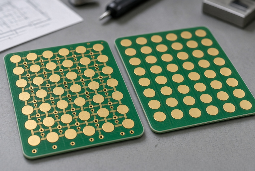
Imagine two boards having the same size of BGA, 0.4 mm or 0.5 mm. Board A will have a via just outside each ball, will employ a short dog-bone and will route the first layer in the channels between the vias. Board B places the via in the pad, fills it and caps it and utilizes the area that was previously the fan out ring for additional nets or for a narrower keep out. These are various routing channels, typology of construction pads and risks of assembly.
Select method from the REAL escape problem. When pitch, number of layers and the size of the via allows for a clean dog-bone pattern, the traditional fan-out is easier. The benefit of via-in-pad is justified by the process steps required if there is no possibility of the package escaping without taking land or if the reduction of that initial hop is a signal and/or density requirement. If the CAD via tool offered it as a default under the footprint, do not pick via-in-pad.
Benefits of Via-in-Pad in High-Density PCB Designs
Via-in-pad is most useful when routing density and small pitch escape is a real constraint. The following are all “trade-offs” between fill, plating, inspection and assembly control. The relationships in this section are not limits on fabricator capabilities – they are only design rules – and should be verified with the stack-up and the shop building the board.
Routing Density and Fine-Pitch BGA Escape
The idea of Via-in-pad for BGA escape and dense routing is to save that dog-bone ring that the conventional fan-out uses. The via is no longer in the channel between the pads, so that channel can be used for another net, another guard trace or just for the clearance that the package had already taken. The first layer switch occurs within the land, not one via-pad away, which contributes to a reduction in fan-out distance.
| Routing item | What via-in-pad frees up | What you still have to check |
| First-layer channels under a fine-pitch BGA or QFN | The dog-bone ring between lands; space that would have held the via pad and its clearance | Residual land area after drill, annular copper, and soldermask opening |
| Fan-out distance off the package | Shorter path from ball or pin to the first inner layer | Stack-up layer pair, via aspect ratio, and whether fill/cap is required for that land |
| Mixed-signal or dense breakout | Room to keep analog, power, and high-speed nets from sharing one cramped fan-out maze | Return path on the reference plane the via lands on after the layer change |
| Component keep-out around the package | Less via crowding at the package edge | Assembly access, inspection, and whether neighboring parts still need traditional vias |
The table is included for planning purposes only and should not be used as a numeric rule. On a particular stack-up, what amount of land and channel is enough depends on the pitch, which is determined by size, copper weight, and the thickness of the dielectric.
Shorter Signal Paths and Improved Electrical Performance
A via in the pad can remove the part of copper strip connected between the ball and the layer change. On high speed nets that shorter path can minimize discontinuity and maintain more of the route along a planned reference plane. The electrical gain only holds if the stack-up already defines that return path. A via-in-pad may be dropped onto the wrong plane or the barrel may be left as a cavity under the land, undoing the layout benefit. This is a placement and stack-up decision and NOT a full high speed design method.
Via Fill, Plating, and Capping Options for Via-in-Pad
Fabricators start the walking on the note in a fixed sequence: filled or un-filled, conductive or non-conductive fill, plating and capping, and the effect of that construction on cost and yield. Filling via the via is not the same as designing a pad. A mean sized land, even if it is perfectly filled, still has a poor solder.
Filled vs Unfilled Vias in Pad
Filled vias seal the barrel, preventing solder from getting in, and the surface can be plated flat. Empty vias leave a “hollow” spot in pad. During reflow that hole draws paste and molten solder into the barrel. When this occurs on a fine pitch BGA via-in-pad land, it typically yields a starved joint and/or a void at the ball.
However, some through-via and test point cases can be constructed with unfilled vias in pad. When it comes to reliability, they are a risk if a tiny SMT land has to accommodate a controlled solder amount, as the hole is under the land. When using a fine pitch BGA and the via is located within the pad, make the assumption that it’s a fill unless the assembly drawing and fabricator both indicate that the open barrel is satisfactory.
Conductive vs Non-Conductive Fill Materials
The most common choice of structure is non-conductive fill. It makes it easier to form a planar land by plating and caps. Does not provide a useable current or heat path within the fill. When a design requires a path for conductive fill to pass through the plugged barrel, it can do so. It is expensive, requires more process control, and is not needed on many signal vias whose sole purpose is to prevent wicking.
Pick the fill from the function of that via. Typically, a signal escape through under a BGA ball requires a plugged, planar land, not a thermal bus. The next note is a power via which is also a soldering surface. With the CAD checkbox, do not set conductive fill on all via-in-pad features.
Plating and Capping for Planar Soldering Surfaces
Once filled, the shop coats the copper with a layer of solder paste and caps the land to create a flat pad for the solder paste to land on. This additional plating and cap is what enables VIPPO to be used on a fine-pitch package. On those packages, a purchasing lead should be prepared for the fabricator to ask about via-in-pad requirements: via size vs. remaining land, fill type, cap planarity, and if the soldermask opening has still matched the footprint.
Thermal vias in a paddle QFN and vias in a metal-core board would be two different heat paths. They don’t call them that just because they’re via-in-pad. These holes too must be filled and capped with a soldering land if they do. The thermal job and the soldering-surface job must be defined as two separate requirements, not that they are the same.
Assembly Considerations for Via-in-Pad
No one source is a controlled note, it’s one controlled note or another. The assembly drawing and fabrication notes should include the pad design (by location on the pad), type of fill, plating/cap, surface finish, stencil intent and reflow caution. If there is control of impedance, the note used in the calculation of the impedance needs to be the same note as reference plane. If appropriate, specify the IPC workmanship class of those joints. Make sure it is “standard via-in-pad” or else the line will not guess it.
One of the most frequent mistakes is a Gerber Set that doesn’t contain a via-in-pad callout, a “filled via” callout in a stack-up PDF and a “unfilled” callout in the quote form. Prefer the drawing. If the construction is altered, give a revision. Please don’t patch the difference in email.
Solder Paste Stencil Design for Via-in-Pad Pads
The aperture of the stencil becomes part of the via-in-pad note since the land becomes a solid copper coin. Fill and cap affect the way that paste is sitting and the amount of solder left after a reflow. Don’t specify the aperture; the printer will assume the default aperture for that package (which is usually the wrong diameter for a via that is capped by land).
| Write this in the assembly data | Do not leave it implied |
| Pad design and via location (via centered or offset in the land; which pins) | “VIPPO on the BGA” with no pin list or land drawing |
| Via fill requirement: filled or unfilled; conductive or non-conductive | A portal checkbox that disagrees with the fabrication note |
| Surface finish on the capped land | Assuming the board finish alone defines the via-in-pad surface |
| Solder paste stencil aperture for via-in-pad lands (reduction, home-plate, or package-default—state which) | “Use standard BGA stencil” with no check against capped lands |
| Reflow profile considerations tied to those lands (paste volume, void risk, package type) | Profile notes that only mention the oven and ignore via-in-pad pads |
| IPC acceptability class for those joints, only if the product requires a named class | “Standard class” or silence when the customer drawing actually names a class |
Reflow Profile and Solder Joint Formation
Reflow doesn’t make up solder volume. When the barrel is open, some of the printed paste will be lost from the land. When the cap is recessed, paste may collect in the dimple and create an empty space between the ball and cap. When the cap is uplifted, it can rock in the package or the joint can wet unequally. When the assembly drawing indicates pointing the process engineer at the lands, the profile should be checked together with the stencil, rather than after the first X-ray of a BGA via-in-pad array.
One owner of the note. If the fill type, cap or stencil is reduced, adjust the drawing and the fabrication package in the same release. A quote form is NOT a drawing.
Cost and Yield Effects of Via-in-Pad That Do Not Show Up in the CAD Tool
Fill, plate and cap are additional process steps, inspection time and the risk of a fine land or a fine space to not yield. The costs are not listed as DRC errors in the layout tool. A board spin can be prevented from the same construction if the original fan-out did not provide a legal path for a fine-pitch BGA. The true comparison is extra fabrication work versus an unrouteable package.
The same amounts of finished vs. started copper, same weights per layer, same via size, same fill type and same minimum space between all lines are the only factors to consider when comparing quotes. A lower cost board that drops the cap, or a higher cost board that provides conductive fill you didn’t expect, is not the same job. Via-in-pad is a designated construction. Do not include the via count in the CAD report and price it as such, but as the construction.
Frequently Asked Questions
What is the difference between via-in-pad and traditional via fan-out?
The traditional fan-out design places the via adjacent to the land and connects to the land with a short trace. In Via-In-Pad, the via is embedded within the pad, which means that dog-bone ring is available for other routing. The first does not require a solid soldering pad and a separate hole. The second approach is to have the soldering pad and the hole be one feature, hence the introduction of the terms fill and cap.
Are filled vias always required for via-in-pad?
No. For the open barrel, fill is required if it is to take solder away from the joint or if it is to create a cavity under a fine-pitch land. If the land, paste volume, and assembly process can accommodate an open hole, then some via-in-pad (VIP) uses in the industry are suitable to remain unfilled. In the case of fine pitch BGA via in pad, it is the usual reliable construction to have either filled or capped. Fill or unfilled should be written on the drawing. Make sure that the fabricator does not assume pick up.
When should I use conductive vs non-conductive via fill?
Plug barrel and present planar land using non-conductive fill. If that plugged via is also meant to conduct current or heat through the fill, then use the conductive fill. Conductive fill is not a quality enhancement. It is not necessary for most signal-escape via-pad lands.
Do via-in-pad designs require special assembly considerations?
Yes. The pad geometry, fill, cap planarity, surface finish, stencil aperture and reflow behavior are all altered compared to a solid land. These are required on the assembly data for the assembler. A via-in-pad BGA is an assembly risk and not a layout convenience.
How should via-in-pad be written on fabrication and assembly drawings?
State in the pad whether and where components and pins to be placed are filled or unfilled, whether they are conductive or non-conductive fill, whether a planar land is needed, plating and cap, surface finish and whether it is a stencil intent. If the class of workmanship is applicable, specify it. Copy the construction into the fabrication notes and the assembly notes. If one of those documents is changed, update both.
When is via-in-pad the right choice, rather than traditional routing?
When there is no escape for traditional fan-out from the package, when the first-layer channels are full, or when a shorter layer change is a known electrical requirement, use via-in-pad. Go back to traditional routing if pitch and stack-up permit a clean dog-bone. The best choice is the one that corresponds to the escape problem and the assembly note that you are ready to control.