A PCB via is a plated conductive path that carries a signal, power, or ground connection from one copper layer to another. It is not just a drilled hole. The barrel, pads, and annular ring turn that opening into a usable layer-to-layer joint. Which of the common PCB via types you should use depends on the layers that must connect, how tight the routing is, the component pitch, electrical behavior, board construction, and what the fabrication budget can support.
A through via that runs the full board thickness is still the right answer for many two-layer controllers and standard multilayer layouts. Blind, buried, microvia, and via-in-pad structures exist because some boards run out of routing room or need a cleaner layer transition. They are not automatically better. They add stack-up planning, inspection work, and cost. Specify them when the layout actually needs them, not because the CAD library offered a smaller hole.
What a PCB Via Does and What It Is Made Of
Before comparing types, it helps to know what you are asking the factory to build. A via is a manufactured connection: a formed hole, a plated barrel, copper pads on the connected layers, and enough remaining land around that hole to survive drilling and registration. Layout software will accept a hole-and-pad pair that a shop cannot plate, register, or inspect. The physical parts of the via, not the CAD symbol, decide whether the connection survives fabrication and assembly.
Via Barrel, Pads, Annular Ring, and Layer Connection
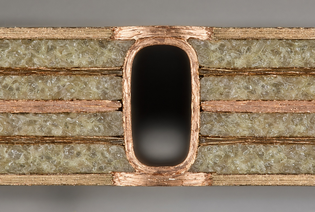
The via barrel is the plated wall of the hole. That wall is the conductive path between layers. Pads on the connected layers give the barrel a copper landing and tie the via to a trace, plane, or component feature. The annular ring is the copper that remains around the finished hole after drilling and registration. If that ring is too thin for the stack-up and drill process, the hole can break out of the pad and leave an unreliable or open connection.
A via is manufacturable only when those parts work together. Hole size, pad size, copper weight, board thickness, and the layers the via is supposed to touch all have to match the fabrication drawing. Accepting a CAD default is not the same as defining a plated connection the shop can build.
Signal, Power, Ground, and Thermal Vias Serve Different Jobs
Via geometry is only half of the decision. Function matters just as much.
A signal via moves a net from one routing layer to another. For faster edges, unused barrel length, impedance change at the transition, and a broken return path can all show up in the same feature. A power or ground via often needs several parallel connections so the current path and the reference plane stay continuous. A thermal via moves heat into another copper area or toward a heat-spreading layer. Keep thermal-via sizing and array rules in the thermal plan rather than treating every small hole as interchangeable.
The same board can mix these jobs. A dense BGA escape may use small signal vias under the package, heavier via groups at the power pins, and a separate thermal array under a regulator. Name the job before you pick the structure.
The Main PCB Via Types Explained
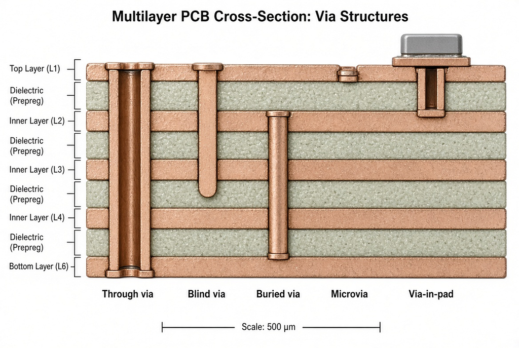
PCB via types are easiest to compare by layer access: which surfaces the via touches, how it is generally formed, what routing problem it solves, and what it costs the build. The five structures below cover most rigid and HDI discussions. They are not interchangeable. A through via on a four-layer industrial board and a stacked microvia under a fine-pitch BGA solve different problems.
Through Vias
A through via runs from the top outer layer to the bottom outer layer. It can connect any intermediate layer the designer assigns, but the hole itself occupies every layer in the stack. Mechanical drilling and conventional plated-through-hole processing make this the default structure on standard rigid boards.
Through vias are the right first choice for two-layer controllers, many four-layer and six-layer designs, and any layout that still has routing channels after the packages are placed. They are straightforward to document and inspect. The trade-off is space. The same hole blocks routing on layers that never needed the connection, and the unused barrel can act as a stub on some high-speed nets. If the board is thick and the hole is small, plating that full depth also becomes harder. That is an aspect-ratio issue, not a reason to abandon through vias on a simple board.
Blind Vias
A blind via connects an outer layer to one or more inner layers and stops before it reaches the opposite side of the board. The usual reason to use one is outer-layer density: a fine-pitch component needs a short path into an internal signal layer or plane, and you want to keep the lower layers free for other routes.
Blind vias require planned layer pairs. The fabricator has to know which outer layer meets which inner layer, and the stack-up has to support that build. That often means extra process steps compared with a standard through-hole stack. Do not specify a blind via only because it looks tidier in the 3D view. Use it when an outer-layer escape or a reference-plane connection cannot be solved with through vias without blocking needed channels.
Buried Vias
A buried via connects only internal layers. Once the board is laminated, the via is enclosed inside the stack and does not appear on the top or bottom surface. That can free outer-layer real estate in a dense multilayer design, especially when inner-layer pairs already carry most of the routing.
Buried vias add lamination sequence and documentation work. The inner pair has to be drilled, plated, and laminated before the outer layers go on. If a standard through-via stack-up can still route the net, a buried via is extra process risk for little gain. Specify buried vias when inner-layer connectivity is the real constraint, and write the layer pairs on the fabrication drawing so the shop is not inferring the build from a drill chart alone.
Microvias
A PCB microvia is a small-diameter via, commonly laser-formed between adjacent layers in an HDI structure. Fine-pitch BGA escape routing and compact modules are the usual drivers. The small capture pad and short layer span free routing channels that a mechanically drilled through via would block.
Microvias are not a generic “smaller through hole.” Layer span, stacked versus staggered construction, reliability expectations, and the fabrication method all have to be agreed before release. A single-level microvia between two adjacent layers is a different build from a stacked microvia that climbs several HDI layers. Do not copy a diameter from another project and treat it as a universal rule. The fabricator’s verified process, not a library default, sets the usable size and stack.
Via-in-Pad
Via-in-pad PCB construction places the via directly in a component pad so the route can leave the land without using a dog-bone trace. Dense BGAs and tight modules use this when there is no room for an escape channel beside the pad.
The assembly consequence is the part that gets missed. An open via in a pad can pull molten solder into the hole during reflow and starve the joint. Filling, capping, and planarizing the via, plus a land pattern that matches that process, are part of the same decision. Treat via-in-pad as a board-and-assembly choice, not a layout shortcut. The details belong in a dedicated via-in-pad discussion; the point here is to recognize when the structure is justified and what it forces you to document.
How to Choose the Right Via Type
Start with the simplest structure that meets the electrical and routing need. Advanced vias earn their place when a demonstrated constraint appears: a blocked BGA escape, a missing inner-layer path, a stub that the signal cannot tolerate, or a pad that has no adjacent routing channel. Cost and cycle time follow the process sequence, so the selection should be written into the stack-up before quotes are compared.
Start With Routing Density and Component Escape Requirements
A two-layer industrial controller with wide parts and open channels rarely needs more than through vias. The picture changes when a fine-pitch BGA, a compact module, or a dense multilayer layout leaves no dog-bone route out of the land pattern.
Walk the escape first. If through vias still leave a legal channel on the outer layer or the next routing layer, keep that stack. If the fan-out blocks every channel, the options are a different layer assignment, a package with a more open land pattern, blind or microvia HDI PCB vias, or via-in-pad. The smallest hole is not automatically the answer. Sometimes moving a net to another layer, or changing which pins share a plane, recovers more room than changing via type.
Consider Signal Integrity, Stubs, and Return Paths
A via is a three-dimensional transition. The signal leaves one reference environment, travels through a plated barrel, and arrives on another layer. Unused barrel below the last connected layer becomes a stub. A missing nearby return via can force the current to detour around a plane split. Neither problem is unique to one via type, but through vias on thick boards create longer unused barrels than short blind or microvia spans.
Identify the sensitive nets before you lock the via map. Ask which layers those nets use, where they change layers, and whether the stack-up and impedance plan already account for that transition. Ordinary GPIO and low-speed control nets usually do not justify a special via build. High-speed pairs and tightly controlled impedance nets do need the transition reviewed with the stack-up, not after Gerbers are frozen.
Balance Fabrication Complexity, Cost, and Production Risk
Blind, buried, and microvia structures can be the correct engineering answer. Their manufacturing sequence is different from a standard plated-through-hole board. Sequential lamination, laser drilling, via filling, and extra inspection all change how the shop plans the lot.
Compare quotes only after via type, layer pairs, stack-up, pad structure, and inspection expectations are aligned. Two “eight-layer” boards are not equivalent if one is through-via only and the other needs buried vias plus via-in-pad under a BGA. A cheaper unit price that assumes the wrong via build is not a saving. It is a delayed engineering conversation.
Via-in-Pad and BGA Assembly Considerations
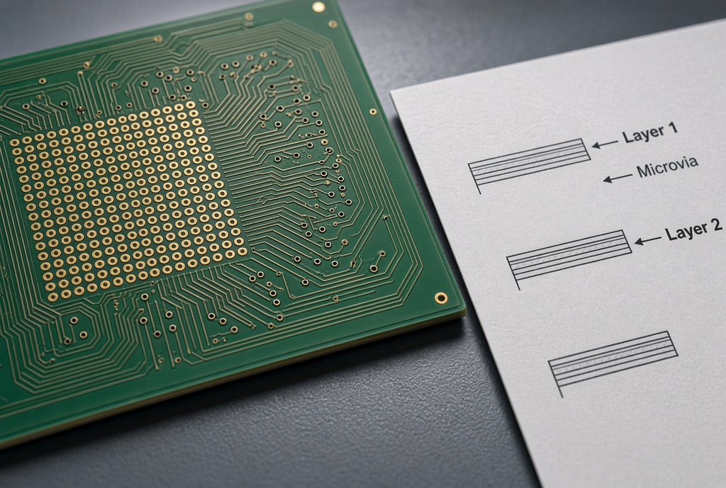
Via-in-pad sits at the boundary between bare-board construction and solder-joint formation. The PCB shop can form the hole and finish the pad. The assembly process still has to put a controlled volume of solder on that pad and keep it there through reflow. If those two plans disagree, the defect shows up as an open, a starved ball, or a void that only X-ray finds.
Why Open Vias in Pads Can Cause Solder Problems
During reflow, molten solder follows the wettable surface. An open via in a pad is a plated barrel sitting under the paste deposit. Solder can wick down that barrel and leave too little metal between the pad and the component lead or BGA ball. The joint may look acceptable from above and still fail electrically or mechanically.
The fix depends on the package, the via location, and the agreed board process. Some designs fill and cap the via so the pad presents a planar solderable surface. Others keep the via offset from the pad when density allows. Copying an HDI footprint onto a standard through-via board without stating how the via in the pad will be processed is a common way to create this problem.
What Designers Should Define Before Releasing Via-in-Pad Files
A manufacturing review needs more than Gerber flashes that happen to sit inside a pad. Include:
- Component package and land pattern, including whether the part is a BGA, QFN, or mixed-technology package
- Exact via locations relative to each pad
- Layer stack-up and the layers each via connects
- Fill, cap, and planarization expectations where they apply
- Finished surface requirement on those pads
- Assembly method and whether the same pads will see solder paste, a BGA ball, or both
- Inspection or test needs for hidden joints
The usual failure mode is a file set that never says the component pads contain vias. The fabricator sees a drill hit. The assembler sees a pad. Nobody owns the solder volume until the first reflow result comes back thin.
Via Design Details That Affect Manufacturability
Via choice shows up in ordinary fabrication data: drill files, pad sizes, stack-up notes, and the fabrication drawing. This is not a universal drill chart. Final hole size, annular ring, and aspect ratio have to come from the chosen fabricator’s verified process. The design task is to keep those inputs consistent so DFM questions happen before material is released.
Drill Size, Pad Size, and Annular Ring
A via needs enough pad land to tolerate drilling and registration variation. Shrinking the pad to steal routing room can push the finished hole to the edge of the copper and raise breakout risk. A smaller hole is not automatically better. It changes plating, registration tolerance, and the remaining annular ring.
Look at hole, pad, copper weight, and layer pair as one set. If the CAD tool reports a legal clearance but the pad looks tight against the drill, ask for a DFM review instead of assuming the default library pad will survive the stack you actually ordered.
Aspect Ratio and Board Thickness
Aspect ratio is the relationship between plated depth and drill diameter. A thick board with a small through hole makes plating the barrel more demanding. Blind and microvia spans are shorter, so their depth-to-diameter relationship is different from a full-board through via.
Do not copy a ratio from another supplier’s capability sheet and treat it as a design rule. Board construction, copper, and the manufacturer’s process set the acceptable window. If the stack is getting thicker and the holes are getting smaller, raise the question in the fabrication notes rather than discovering it after the first panel.
Fabrication Drawings and Stack-Up Notes Must Match
Conflicts usually look like this: the Gerber drill file shows a through hole, the stack-up sketch calls for blind vias, and the fabrication drawing never names the connecting layers. The shop then has to guess which document wins.
One controlled package should identify via types, layer pairs, drill requirements, and any special notes for filling, capping, or sequential lamination. Revision-controlled outputs keep the layout, the stack-up, and the drawing on the same change. If those three files disagree, stop and align them before the quote is treated as final.
Common Via Design Mistakes to Avoid
Most via problems are specification problems, not mysterious process failures. The mistakes below show up repeatedly in file reviews.
Using Advanced Vias Before Checking Whether Standard Routing Works
Blind, buried, and microvia structures should solve a demonstrated layout or performance problem. Route the board with the simplest viable stack first. Mark the nets and packages that still cannot escape. Then review advanced structures with the fabricator against that constraint.
Starting from an HDI via map “because the package is small” often adds lamination steps the design never needed. The extra process does not improve a board that still had routing room on a through-via stack.
Treating Via-in-Pad as a Layout Shortcut Only
Via-in-pad changes how solder forms on that land. If the files do not define fill or assembly expectations, the board and the assembly line are working from different assumptions. Copying an HDI footprint into a standard board file without those notes is the usual path to starved joints.
If the package can escape with an offset via and a short dog-bone, that is often the more controlled choice. Use via-in-pad when density leaves no other legal path, and write the process into the package.
Leaving Via Type and Layer Pairs Out of the Fabrication Package
A drill chart lists hole sizes. It does not, by itself, define a blind or buried via build. Include a controlled stack-up, named layer pairs, fabrication drawing notes, and revision-controlled outputs. Engineering questions belong in that package, not in an email after the material is already on the press.
Questions to Ask Before Finalizing a Via Strategy
Use this as a review between the designer, the purchasing lead, and the manufacturing partner before a quote or DFM cycle. The goal is to name the actual problem and the build that solves it.
Design Questions
- Which nets must change layers, and which layers do they use?
- What is the tightest component pitch, and does any BGA or module lack an escape channel?
- Which signals are fast enough that via stubs and return paths need a review?
- Are there thermal vias that belong to a heat path rather than a signal path?
- How much routing area remains after the packages are placed on the current stack?
Answer those before choosing a via type. Density, performance, heat, and land pattern each point to a different structure.
Manufacturing Questions
- Are layer pairs for blind or buried vias named on the stack-up?
- How thick is the finished board relative to the smallest through hole?
- Do any pads require filling, capping, or a planar surface?
- What inspection is expected for hidden joints or sequential structures?
- Does the board need sequential lamination or another special process, and is that process agreed?
Ask the chosen fabricator to confirm the process against the files. Do not treat another shop’s capability list as the rule for this build.
File Package Questions
- Do Gerber or ODB++ data, drill files, stack-up, and the fabrication drawing describe the same via types?
- Are impedance notes, if any, consistent with the layer transitions?
- If the board will be assembled, are the assembly drawing, BOM, and centroid data included, and do they mark via-in-pad lands?
- Is the package revision-controlled so a stack-up change cannot drift away from the drill file?
Complete files reduce the gap between bare-board fabrication and BGA assembly planning. Incomplete files force each group to invent the missing note.
Frequently Asked Questions
What is the difference between a through via and a blind via?
A through via is drilled through the full board thickness and can connect any assigned layer along that path. A blind via connects an outer layer to one or more inner layers and does not reach the opposite side. The through via is simpler to build on a standard rigid stack. The blind via preserves routing space on the layers it does not enter, at the cost of planned layer pairs and a more involved fabrication sequence.
Are buried vias always more expensive than through vias?
Not as a universal rule, but they usually add process steps. A buried via is formed on an inner pair and then laminated inside the board. That sequence, plus the documentation and inspection it requires, is more work than a standard through-via stack. If through vias can still route the design, the buried structure is rarely the cheaper path.
When should I use microvias instead of standard drilled vias?
Use microvias when adjacent-layer connections and fine-pitch escape routing cannot be solved with mechanically drilled vias without blocking channels or forcing oversized pads. Compact modules and HDI PCB vias are the common case. Agree on layer span, stacked or staggered construction, and the fabricator’s process before release. A microvia is not a drop-in replacement for every small through hole.
Is via-in-pad required for every BGA package?
No. Many BGA land patterns still escape with dog-bone traces and vias outside the pad. Via-in-pad is justified when pad pitch leaves no legal channel beside the land. It should be specified with the fill, cap, and assembly notes that protect the solder joint, not applied to every BGA by default.
Can open vias in pads cause solder defects?
Yes. Molten solder can wick into an open plated hole and leave too little solder on the pad. The result can be a starved BGA ball, a thin QFN joint, or a void that is not obvious in a top-side visual check. Filling, capping, offsetting the via, or changing the land pattern are the usual controls. The right control depends on the package and the agreed board process.
What files should I send for a PCB with blind or buried vias?
Send a consistent package: Gerber or ODB++ data, drill files, a stack-up that names layer pairs, a fabrication drawing that states via types and any special notes, and revision-controlled outputs. If the board will be assembled, include the assembly drawing, BOM, and centroid data, and mark any via-in-pad lands. A drill chart alone does not define a blind or buried build.