The copper conductors that transport the current and signals between pads, via’s, and planes are called PCB traces. The width, spacing and copper thickness are not designating each other. They relate to etch, plating, impedance, voltage clearance, and the density of routing a layer. Select them as one geometry package and the board will be more likely to etch cleanly, the impedance model will stick to it, and the board will be assembled without shorting.
It’s assumed that any width and spacing will do once the router has done its job. If that’s how you get them, they show up as drawn width, inner layer and outer layer in the same space, and no note to CAM what weight copper is the start of the foil and what is the end of the foil. The width, spacing and thickness must be selected simultaneously and the fabrication drawing must indicate this.
PCB Traces: What Width, Spacing, and Thickness Actually Mean
In production language, trace geometry is a set of three measurements, not a CAD property. The copper conductor is width. Spacing is the space between conductors, pads and pours that is not occupied by copper. Thickness is the thickness of copper after processing. All three of those terms and an impedance calculator will use different numbers, as will an estimate of the current and a CAM review.
Trace Width as Drawn vs Finished Width After Etch
The dimension that is measured in the copper layer (Gerber or OBD++). Finished width is the width after etch and after plating on outer layer. Etchant will attack the sidewalls. For plated outer, the starting foil typically is thinner than the end result, and the etch profile will not be identical to an etch in an inner foil.
The actual problem is to use the width of the drawn conductor instead of the finished conductor in a calculation of impedance or current. When CAM uses etch compensation, the end result is a line that is close to the drawn line number. Without any compensation, or with heavier copper, the actual width is frequently less than the CAD width. Record the number the design means. If not, the fabricator is working on a different board than the SI model.
Trace Spacing as Cleared Copper, Not Just “Gap Between Lines”
The distance between the traces (spacing) after processing is called PCB trace spacing, which does not necessarily correspond to the copper-to-copper distance, nor to the distance between the soldermask openings. There are two different layouts that can be the same drawn gap and be different jobs. One designer sees the space as just clearance for dry film etching. The other one also requires a soldermask dam to be added between pads or between a trace and pour. These are different shorting risk, different yield, and usually different process windows.
Make a statement regarding spacing in the design notes: copper to copper, copper to pour, copper to edge and mask dam or not. If a number is in a CAD constraint set and is not labeled with a unit and has no “drawn or finished” label, it is not a fabrication rule. It’s a wish that CAM will get it right.
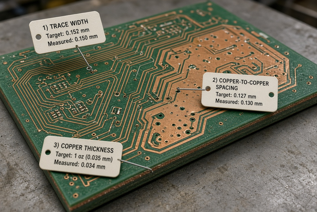
Trace Width, Spacing, and Thickness: The Practical Relationship
Width, spacing and thickness go hand-in-hand. Clearance, temperature rise and current models and curves are provided in IPC documents. Those models are not one geometry that is correct, nor can they replace the stack-up and the process window of the fabricator. The numbers below are suggested thinking numbers, not process limits nor a copy of the standards table.
How Copper Thickness Drives Minimum Spacing More Than Width Alone
It is a matter of thickness, NOT width, of copper that determines the ease with which a space will etch. There is a difference in etch problem if the gap is next to thin foil versus the same gap next to a plated or thick copper feature. The copper becomes taller and sidewall etch, undercut and register all increase with increasing copper height.
| Copper thickness (guideline) | What usually happens to spacing | What actually changes the spacing |
| Thin starting foil on fine-line inner or impedance layers | Tighter copper-to-copper gaps are more realistic because the etch depth is smaller | Drawn vs finished width, etch compensation, and whether the gap is copper-only or also needs a mask dam |
| Standard finished copper on mixed digital layers | Spacing is driven as much by routing density and pad clearance as by the trace itself | Annular ring, via-to-trace gap, and whether inner layer and outer layer traces share the same constraint set |
| Heavier finished copper on power or high-current features | Spaces usually need to open; tall copper is harder to etch cleanly between close features | Pour-to-trace gaps, copper-to-edge, soldermask coverage over thick copper, and registration to the drill |
| Mixed thin signal and thick power on the same layer | The fine space next to the heavy feature becomes the yield limiter | Local copper balance, thermal reliefs, and whether the heavy feature should have been a plane or a thicker stack instead |
The thickness of the trace does not dictate the width of the space. A thicker conductor typically does. Review the relationship against the stack-up, starting foil and the fabricator’s etch process, not recreate the same constraint for each layer.
Inner Layers and Outer Layers Do Not Etch the Same Way
Inner layer traces are made of copper foil over a core. This foil is cleaned, patterned and etched. Thin foil outer layers are typically used and then plated up in the holes and on the surface before the final etch. A note indicating 1 oz; with neither a starting or finished note, nor any inner or outer note is hiding that split.
If one side of a drawn PCB trace is foil-etch and the other side is plated-then-etched, the same trace that is drawn will not end up the same conductor. It is a common occurrence that a board designed to look fine in CAD is returned with various questions about etch or impedance because outer-layer spacing has been copied to the inner layers or vice versa. Assume that there are two process families, inner layer and outer layer, that share a stack.
How to Choose Trace Width, Spacing, and Thickness for Your Board
The routing of the PCB traces is done in the order a reviewing engineer will perform it and not in the order they are finished by the router. The first priority on power paths are current and allowable temperature rise. The next step is voltage drop on a long rail, then heat spreading, then impedance and loss on controlled nets, and finally etch and cost. A wider trace cannot replace a plane, heavier copper weight or thermal path via- or metal-core construction.
When Standard Widths and Spacings Are Enough for Digital and Mixed-Signal Boards
For many 4-layer digital or mixed-signal boards, a standard width and spacing for the signal layers is sufficient. Thin starting foil, also known as thin inner foil, is frequently used when the fine etch and impedance are more important than the rail current. Power requires either a plane or a purpose-made sized pour. Avoiding locking of inner signal layers to the outer-layer geometry because that constraint class already has it.
When you have mostly modest speed digital boards and short runs and generally a good reference plane, there is little point in being aggressive about geometry unless you are looking for a tough CAM review. Fill the “densities” or “impedance” needs with the nets and keep the rest within an “etch window.”
When Wider Traces, Tighter Spacings, or Heavier Copper Are Justified for Power and Impedance
Wider traces are warranted on higher current where voltage drop is important on some heat spreading paths, and on long rails. With dense BGA escapes, fine pitch routing and certain controlled impedance pairs where it may be necessary to keep them in a narrow line, tighter spacings are warranted. When the current or thermal load is no longer a trace problem, heavier copper is warranted.
The three requests are not equivalent. Don’t mistake a wide trace on standard copper for a heavy copper power board. Migrating to 2oz finished copper and higher typically results in a longer etch, wider spaces, increased stress in registration and hard soldermask window over tall copper. Don’t include heavy copper on all layers as one rail was hot in simulation. Place additional metal in the place where the existing metal is located.
Impedance acts in contrary manner with brute force current. The material of the copper in the impedance model must be the same as copper in the finished (or compensated) conductor on that layer. After the stack-up of the PCBs is frozen, changing the thickness of the copper changes the line width that achieves the target impedance and the loss on the line.
What Gets Harder as the Trace Geometry Becomes More Aggressive
When traces get narrower, spaces get tighter or copper gets thicker, three things typically get less comfortable: minimum space after etch, solder mask dams between features and impedance tolerance. The fabricator should ask the purchaser if they have a fine-pitch escape on the same layer as a heavy power pour adjacent to it. The warning is not a software warning. It’s a battle of two process windows for the same space.
Thermal via and metal-core boards are two distinct heat paths. They don’t sit on a typical FR-4 stack as “extra ounces of foil”. If it’s not the heat getting out of the board, do change the thermal path. Avoid fattening all traces.
How to Specify Trace Geometry So Fabrication Does Not Guess
The note is the foundation upon which CAM can be built. The minimum information that needs to be included in the fabrication data is the name of the layer, starting foil or finished copper, weight or thickness, and if there is a difference between the inner and outer layers. If the impedance is controlled, then the copper should be the same in that calculation as it is in the note. If IPC acceptability class is relevant, use the name of that class. Standard Copper is a not a class or a thickness.
Callout Matrix for Trace Geometry Fabrication Data
| Write this in the fabrication data | Do not leave it implied |
| Inner-layer foil weight, per layer or per core | “1 oz throughout” with no inner/outer split |
| Outer-layer finished copper, or starting foil plus finished target | A portal field that disagrees with the stack-up PDF |
| Units when thickness is given in μm or mil, not only “oz” | A number with no unit next to a mixed oz / mil drawing |
| Impedance-model copper when impedance is controlled | A line-width table that never states drawn vs finished copper |
| IPC class only if the order actually requires it | “Standard copper” or “normal quality” as a substitute for a class |
| Copper-to-edge, heavy-pour, and mixed-weight notes that change etch | A Gerber set with tight spaces next to an undocumented thick pour |
Trace geometry for PCB design is complete when that matrix is congruent in all three documents, the stack-up, the fabrication drawing, and the quote package. In case those three sources are not in agreement, production will follow one of them and you will not know which.
Where the Trace Geometry Note Should Live
Put the controlling note on the stack-up and the fabrication drawing. Email snippets and quote form dropdowns are bad teachers. Typical failure is a Gerber that contains no geometry note, a stack-up PDF that indicates an 1 oz finished and a portal field that indicates 2 oz. CAM has three answers but no revision flag.
Use one controlled note. If any of the above factors change, give a revision. Avoid the patching of the change in a later email and do not leave the drawing unattended. The drawing will be the one that will be left on the shop floor after the email.
Cost and Yield Effects of Trace Geometry That Do Not Show Up in the CAD Tool
The higher the weight of copper, the more expensive the foil and the longer it will take to etch it. It can also increase the likelihood of an unyielding fine space, particularly when located adjacent to a dense signal channel and a power pour. If the original geometry were never intended for the current or for the drop, the same change will prevent the board from spinning.
The autorouter generates tighter spacing which appears free. In the shop it uses process window: etch uniformity, soldermask dams, registration and inspection. When the layout could have been laid out by one of the two processes, the same layer is often over-used with both of them, thus costing more money than needed.
The quotes made only after starting versus finished layer weights and the minimum space are the same. A lower number which would use thinner foil or a wider space does not equate to the same board. Commercial check is a part of the basics of PCB trace routing. The CAD canvas will not make it for you.
Frequently Asked Questions
Is trace width the only factor that sets current capacity?
No. The current capacity is dependent on the finished thickness of copper, whether inner or outer trace, the allowable temperature rise, the proximity of nearby copper to spread heat, and length of run. Width is one input. A “wide enough” rail still runs hot because it’s treated as the only input.
What is the difference between trace width and trace spacing?
Conductor is width. Space is the space in between conductors and other copper elements. The width is used to determine the amount of metal that carries the current or holds the impedance. Spacing sets define risk, voltage clearances and if a soldermask dam exists between features. They are given together since they are both removed by the action of etch.
Should every layer use the same trace width and spacing?
Typically, no, inner layer and outer layer traces do not etch the same and do not perform the same function. There have to be constraints for impedance layers, escape layers, and power layers. One might think that copying one class across the stack would make them invisible until they are brought to the surface by CAM or the first article.
Does a wider trace always carry more current?
The wider the trace on the same layer type the more current that can be carried for a given temperature rise. It is NOT the same as a heavier copper or plane or a short wide pour in a plane. The length remains a factor, drop is still a factor, heat spreading is still a factor and inner or outer copper is still a factor. You don’t want to waste routing density that might be required later by opening up all of your nets “just in case.”
How should trace geometry be written on a fabrication drawing?
Identify the layer, starting foil / finished copper, the units and if there is a difference between inner and outer layers. If the model is controlled for impedance, indicate the copper used for the model. If it is a required class, please specify the class name.
When is a heavier copper PCB the right question, rather than tighter spacing?
Request thicker copper where continuous current, voltage drop or heat spreading has exceeded the capabilities of a standard weight trace or pour. Tighter spacing is not an upgrade, it’s a density and clearance issue. If the layout is attempting to place fine geometry and heavy copper on the same layer, break it into separate components—put the fine geometry on a weight that can be etched, and the current in a plane, wider pour or a layer that can support the metal.