Doing so is not an option for multi-layer PCBs. Core is a fully cured material with copper on one or both sides with a dielectric quality. Prepreg is a partially cured resin-reinforcement sheet which can be flowed and bonded during the lamination of those cores. Treat them as the same material, you have an effectively wrong thickness of the dielectric, have an incorrect target for the impedance, and will send a stack to the fabricator that they can’t fabricate as drawn.
They both appear to be “the insulator between copper”. They are not substitute for each other. Core does not have a tendency to alter its shape. The thickness of the prepreg after lamination will depend on the amount of resin used, the number of plies and the compression of the plies in the lamination press. This guide is intended for hardware engineers, PCB design engineers or SI/PI or NPI that must place each material.
What Is a PCB Core?
PCB core is used to construct the multi layered stack which is a stable structure. If it is used in inner layer process, it will be cured and the thickness of the dielectric will be the initial value of the process.
Structure and Manufacturing Role of Core
A core is a cured laminate (resin and reinforcement in the form of most usually woven glass) covered on one or both sides with copper foil. It is bought in certain dielectrics and copper weights by the fabricator. The cores are then covered with prepreg then pressed into a solid board, and the circuits to be created on the inner layers of the board are then imaged and etched on the copper.
The resin in a core material is cured before it is used in the manufacture of the core product. Can hold up its thickness in lamination, and can give a reference plane on top of the stack. This is because cores are not the glue that is used to hold the blocks of the multilayer together, but the core blocks of the multilayer.
Where Core Appears in Typical Multilayer Stack-Ups
In most multilayer constructions cores are used to connect signal and reference layers. A typical construction consists of two layers of copper foils with a middle insulating layer (dielectric) between them. Cores are also used to achieve a predictable dielectric for impedance when such is required by the designer, between a signal layer and a nearby plane. If the desired thickness of the finished board is known, and sufficient number of prepregs cannot be stacked to reach the desired thickness, then more cores will be used.
As the main inputs for layer planning, copper weight and core thickness are used. The later the values are changed the greater the impedance, the registration and the overall thickness. Doing cores first, and “bond and tune up” with prepreg.
What Is Prepreg, and Why Is It Needed?
If the cores are separated, the bonding layer is known as prepreg. It is very important that it is not in place, otherwise, etched cores would be loose sheets.
Prepreg as Partially Cured Resin-Reinforcement
As a reinforcement, prepreg is a partially cured (B-stage) material comprising of glass cloth or other reinforcement material soaked in resin. In the case of the press, this resin flows into gaps and passes around copper under heat and pressure, and is completely cured. This develops a bond line between cores.
The importance of a prepreg sheet is not that it will be a certain thickness. After lamination, the thickness will be determined by the amount of resin used, the number of plies between two copper layers, the density of copper pattern and the press parameters. The prepreg thickness of the PCB design is not simply a value you can throw in an impedance calculator and get on with it, it’s a value which needs to be verified with the fabricator.
How Prepreg Enables Multilayer Construction
Prepreg performs 3 functions in 1 lamination cycle. It is a link between the adjacent cores. No voids will be left between layers with it. It can also be used as a dielectric between some pairs of layers and thickness to the finished boards.
Core and prepreg in the construction of PCB need to be planned in the following three jobs. Even a stack that is perfectly good on a drawing may not be good if the prepreg does not flow to the desired dielectric or the press cycle the fabricator has does not meet the requirements.
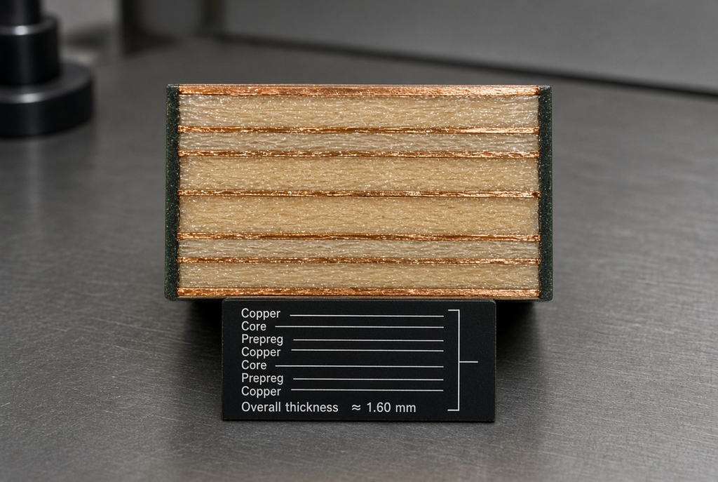
Key Differences Between Core and Prepreg in Stack-Up Design
What’s helpful for the comparison is not, which material is better. The type of job, each one can reliably perform in a multi-layer stack-up.
Thickness Control and Dielectric Consistency
The thickness of the core is predetermined in the laminate mill and is fairly constant during inner-layer processing and lamination. Therefore, core is a better choice than prepreg if it is required to have a specific thickness, especially in the case of controlled-impedance layers.
Once the prepregs have been laminated, their thickness will be a process result. Resin tends to migrate towards low copper regions, and away from high copper densities. Multiple thin plies can be stacked together to achieve a desired value, but the resulting value still falls within a window. Impedance-critical dielectrics are thus frequently used opposite cores. A range of prepreg is used to bond those cores and some rethickness is added with a prepreg (assumed to be a range).
Mechanical Behavior, Warpage, and Symmetry
The cured core is stiffer than a prepressed core of the same thickness. After being laminated together, they are both composited, but the order of the lamination makes a difference. Heavy copper on one side of the panel, extra prepreg on the other side of the board or cores clustered at the top of the board can cause the pull on the panel during cooldown.
It is that imbalance that is likely to lead to warpage in a multilayer PCB stack, not a particular “bad material”. Even core and prepreg distribution and mirrored core/prepreg configuration minimizes bending moment after press and after assembly reflow. Mixed-Signal or Power Boards do not always need to be perfectly symmetrical, the goal is to have a small mismatch to ensure that the panel stays flat throughout the depaneling and SMT process.
Thermal Behavior and Lamination Considerations
Core has the resin completely hardened. It is stable when in the press. A prepreg resin is required to flow into the copper without failure, to wet the copper, and to be completely cured. When the stack is too dry, too wet, or when the heat-up rate is too fast, voids and/or resin-starved glass may form in the bond line.
The difference is what makes fabricators want to know what they’re putting in the stack before committing. They’ll have to determine which layers are cores, how many prepreg plies to add in between, and which copper weights to fill. A Finished Thickness drawing with no core/prepreg sequence will let the shop decide which thicknesses to use, and that may be different from the thickness you used for your simulation.
How Core and Prepreg Affect Impedance and Signal Integrity
The electrical performance is associated with the placement of dielectrics. The material between the trace and reference plane will have a greater influence on the impedance, rather than the material two layers apart.
Choosing Dielectrics for Controlled Impedance Layers
The planning of controlled impedance core and prepreg starts from the reference. Typically, microstrip has a solder mask and the outer dielectric, while stripline is between two planes that are separated by a defined dielectric. Those dielectrics that are most critical are usually employed in the core, because the core thickness is a more certain number.
In fact, up till today prepreg is employed in almost all impedance stacks. It’s employed for connecting the core pair to the other components of the board and can be applied as part of the dielectric on top and bottom of a stripline. This impedance model of the fabricator should include the thickness of the core, Dk of the core and the thickness of the prepreg to be pressed, with the Dk for the number of plies of prepreg. The first lot consists of tight boards, obtained by requesting a model based on “nominal prepreg only”.
When Prepreg Thickness Variation Becomes a Real Concern
Variation is an insignificant issue for a thick capacitance/dielectric that has a broad impedance window. A concern in a thin dielectric and tight tolerance and high speed, or RF channel. Under these circumstances, a few tenths of a mil of added flow will be enough to trigger a late change for the stack or trace width.
Inform the Impedance budget from early stage. When the design is only usable when the prepreg is applied at one given thickness, the stack is over-determined. One approach is to set the window’s electrical requirement (target impedance, layer pairing, window allowed), and then leave it up to the fabricator to recommend a core/prepreg combination that they can use in the window.
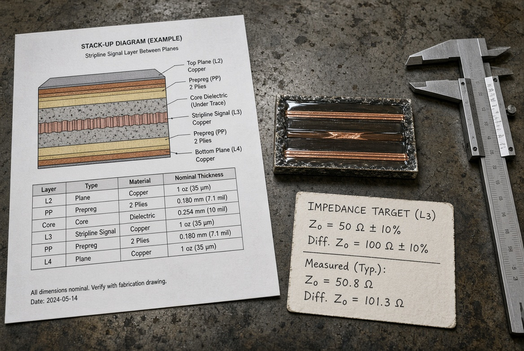
Common Pitfalls When Using Core and Prepreg in Multilayer Designs
Most of the stack-up problems are not uncommon. They are associated with seeing a process as a given size, or with the freezes a construction that the shop cannot work.
Treating Prepreg Thickness as a Fixed Number
The most common error is to call a prepreg designation in the impedance tool, as though it were a completed core. This happens later: When the measured impedance is correct, but the last minute request is to change the geometry; or when the thickness pressed does not match the thickness on the drawing because of a fabricator note.
Build up the model with the presses’ thickness range, and compare the range to the shop’s data for this specific number of plies and copper style. If the circuit design is not able to handle the range, then change the critical dielectric to core, or decrease the electrical window.
Unbalanced Stacks and Warpage After Lamination
Another common error is to stack cores, prepregs and copper for ease of handling the circuit without considering mechanical symmetry. If there is a heavy copper plane on one of the sides, a thick core at the top, and thin prepreg at the bottom, it will be bowed when press and reflow.
That bow, isn’t a make up bow. It presents as assembly difficulties, solder joint geometry variations and extra stresses on through-hole during thermal cycling. The stack should look like a sandwich, that is, similar amounts of copper should be on either side of the center of the board (unless there is documented mechanical constraint).
Over-Constraining the Stack Without Fabricator Input
One possible pitfall is to set all core thickness, all prepreg ply and all glass style before materials review. Some combinations might not be offered. Some of their stock is qualified, but not qualified for that copper weight, that press cycle. It’s not a rework, it’s a redesign, after the quotation, not before.
Pass electrical/mechanical requirements: number of layers; layers that need impedance control; board thickness window; copper weights; any symmetry/reliability notes. Discuss the proposed core and prepreg sequence with the fabricator. In some instances, custom stacks are needed. They are to be a reaction to a true limitation and not a first draft.
Practical Stack-Up Planning With Core and Prepreg
One approach is to determine the general actions that the board needs to take, and then pick multilayer PCB stack-up materials that can be constructed.
Start From Electrical and Mechanical Requirements
It is best to start with the number of layers, whether these are impedance controlled layers, layers, final thickness, mechanical limits, such as bow/twist, and keep out from connectors. The selection of core and prepreg materials meet those requirements. They are not an exercise in materials per se.
Prior to naming a prepreg, write the reference structure for each impedance layer. If the stripline needs to be installed between L3 and L5, choose the material that will be used as the bottom layer of the stripline (the choice of core, pressed prepreg group, or a combination). After that it’s all downhill.
Use Standard Core/Prepreg Combinations Where Possible
Available stock of previously characterized lamination and impedance fabricators’ standard core and prepreg combinations. Today they’re no longer “fashionable” constructions, they are here because they are effective! They are to use them as the first proposal. Employ the standard set of thickness, impedance or reliability unless there are special needs for customization.
The stack-up design of PCBs is a practical matter, and the prepreg is able to be stacked up with the core in a number of ways:
- Set freeze layer targets and set the function of freeze layers.
- Use cores to cover most sensitive dielectrics.
- For the remaining thickness use the minimum number of prepreg groups the shop will hold.
- Test copper & dielectric symmetry in the midplane region.
- Return the improved stack to the fabricator for a qualified replacement if it will fit in the electrical window.
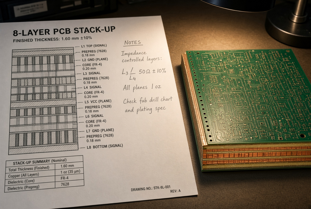
Summary Guidance – Treat Core and Prepreg as Complementary Tools
Core and prepreg are not synonymous terms, they refer to two techniques in the process of making a multilayer printed circuit board. Apply cores for stable dielectric blocks and as the main location of tightly controlled impedance layers. These cores are bonded together by filling the copper relief with prepreg and adjusting the thickness of the relief.
Sharing the stack with the fabricator as long as the design is still changing. An electrically sound construction that is pressable will pass prototype and NPI and repeat builds. The construction which only works if prepreg lands on a certain number will not work in general.