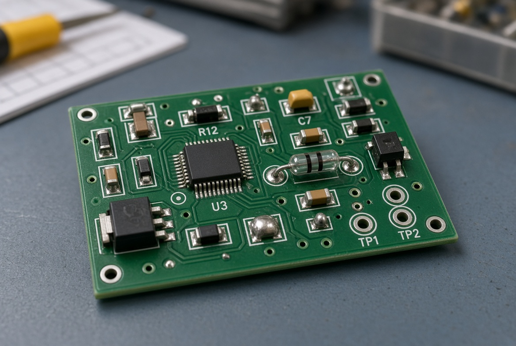
PCB silkscreen is the legend that is printed on a finished board to provide assembly, test and service teams with the knowledge already known by the CAD file. It’s a functional layer, not for marketing copy or decoration. These problems include operators mistaking parts as being placed backwards, missing or overcrowded layers, and probes resting on ink rather than copper.
It is an easy and expensive mistake to make to consider silkscreen optional. The electrical netlist may be correct and the board may still fail on first article inspection for a number of reasons: Some diodes do not have a cathode mark on the device or board, a connector does not have a pin-1 cue, or the revision exists only on an internal drawing. The rest of this guide explains what the PCB legend layer is used for during production, how it differs from solder mask, and the PCB silkscreen production mistakes that crop up on the line.
What PCB Silkscreen Is Used For in Real Production
No one’s looking at your schematic in an SMT line or on a through-hole bench or a field-service kit. They are examining the board. But, once the copper and the mask are done, the only one that speaks that language is silkscreen. When the legend does not contain the information that these people need, the assembler makes a guess, the test person scans through a pdf and the next revision is indicated by a handwritten mark rather than a controlled mark.
Assembly: reference designators, polarity, and orientation
When two 0402 capacitors are placed within a few millimetres of each other, reference designators provide information to the operator to distinguish C17 from C18. They help them know the cathode or the positive terminal on a diode, tantalum or electrolytic capacitor. Pin-1 indicators on ICs, headers and board-to-board connectors prevent an incorrect 90° or 180° placement, which electrical test might not detect until the board is complete.
All of this is already displayed on screen in CAD. The shop floor doesn’t. One of the most frequent errors is to forget to include the polarity and pin-1 indications in the legend since “the pick and place file contains rotation.” The file is handy for the machine. It does not help a hand-placing technician for a through-hole connector which has to be inserted at the last minute, or an inspector who is checking first article against the assembly drawing. The assembler will only “know” the polarity until a shift change if it is not on the board.
Use the simplest markings for each component based on the component datasheet; polarized capacitors are marked with a stripe, diodes with a cathode bar, pin 1 with a dot or “1”. A QFN and a nearby header are rotated in opposite directions when a mix of three different pin-1 conventions is used on one board.
Test, service, and revision tracking
Test-point labels and connector function names, and board part number and revision should be on the PCB legend layer for the same reason that designators are: the person holding the board should not have to open a private folder to find out which unit they have. Wrong-probe events are reduced by clearing test labels. Connectors are given names like J2 / USB or P3 / FAN to reduce time when the fixture (or field cable) is connected to the wrong header.
Revision and part numbers are only printed in an internal drawing to aid with document control. They are not of assistance when someone is getting a board, when it comes to a first article inspection, or when the receiving team has two nearly identical boards on the bench. Secondary elements are date codes and manufacturer logos. When space is limited, you can save revision/part number and omit the decorative mark.
Silkscreen vs Solder Mask: Different Layers, Different Jobs
Fabrication notes that designers write assuming they have to deal with two colors of drawings, silkscreen and solder mask, are notes that cannot be respected by the process. The two layers are stacked on top of each other. They don’t perform the same duty.
Solder mask defines solderable openings; silkscreen marks the board
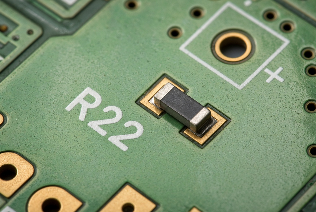
Solder mask is the coating that reveals copper for solder to wet (pads, test points and designated contact features) and protects copper that should remain protected. On top of that mask is the non-conductive ink which is used for silkscreen printing the text and symbols. Is not an electrical opening definition. It is not intended to replace mask clearance, paste opening or a keep-out.
The common mistake is to draw legend on a pad and presume that the mask will solve the problem. When you release the Gerber layers, they will be used as the basis for fabrication. If the silkscreen aperture touches a pad, ink will deposit on that pad (unless the fabricator clips the artwork—which is a subjective determination and not a sure thing that the text you want is present).
Why silkscreen on pads and test points causes problems
When soldered on a solderable pad, ink on the pad will decrease wetting, leave a residue on the solder joint, and make visual and AOI inspection more difficult as the pad will no longer appear as a clean copper or finish surface. A test point can be coated with ink and the metal may be under the test point. A flying-probe or fixture pin on the legend rather than copper results in an intermittent contact, appearing as a test-program error.
Do not place silkscreen on any solderable surface, or any desired probe landing. Remove the designator or drop the character if there is no other destination for the designator other than the pad. Avoid putting a logo on a test coupon or bed-of-nails landing.
Practical Silkscreen Design Rules for Assembly and DFM
The readibility of the legend after the board is built is more important than an over-detailed CAD drawing. DFM for PCB Silkscreen is primarily about text that does not change when it is viewed and processed, and clearance that doesn’t allow ink to compete with copper, mask or mechanics.
Text height, line width, and readability after assembly
A 4K monitor looks great at 400 percent zoom size when displaying very small text. In a completed circuit board placed under a bench lamp, the same string turns into a grey pad, particularly when solder mask texture, some print offset and a high component are placed next to it. Line width too thin is a problem of the screen, or the inkjet process, and too heavy fills closed characters like 8, B, 0.
If there were such a thing as a universal minimum that all fabricators and all density classes could publish as a universal rule of thumb in this article, then this text would be devoid of value. The height and stroke of the text will vary according to the print method, board density and fabricator’s process window or tolerance. Request that window before locking 0.5 mm characters in a dense analog segment. Even if the text fits the courtyard in CAD, the assembler may not be able to read the designator after the part is placed, so the text didn’t do its job!
Prefer short strings. “C14” beats “CAP_FILTER_INPUT_14”. Orientation should be in the same direction as the reading direction of the rest of the board otherwise inspectors will need to rotate the panel for each line.
Clearance to pads, vias, and board edges
The first DFM check to prevent the above-mentioned ink-on-pad issue is called silkscreen clearance to pads. Avoid placing legend on SMD pads, through-hole pads, exposed vias serving as test points, or tooling/fiducial copper. Any part number on the edge of the board will be lost when routing, scoring and handling; a part number placed on the breakaway tab is lost after depaneling.
A second, silent failure is a designator that is placed close to a component body so that when the part is soldered, it obscures the designator. The placement of reference designators on a PCB should take into consideration the completed layout. Pull the string in 1 open area of mask that will show through after the package has been down.
Placement that survives component height and viewing angle
Think of the board in the eyes of an assembler or technician: from above and a bit off-center, connectors, shields and high electrolytics are already in place. During first-article or rework, legend under a right-angled connector, under a shield can or in the shadow of a heatsink is not available.
Locate critical marks (polarization, pin 1, fuse rating, safety warnings for high voltage products, etc.) for easy viewing by user standing at bench while not removing hardware. Do not place test labels on the other side of a high part. When both sides are installed, install each designator on the side that the component is installed on, unless your assembly drawing specifies otherwise.
Common Silkscreen Mistakes That Cause Assembly and Service Issues
The majority of PCB silkscreen errors are layout practices and not any extreme process limit. They manifest themselves as additional rework, delayed inspections and boards that require the original CAD session to be open for service.
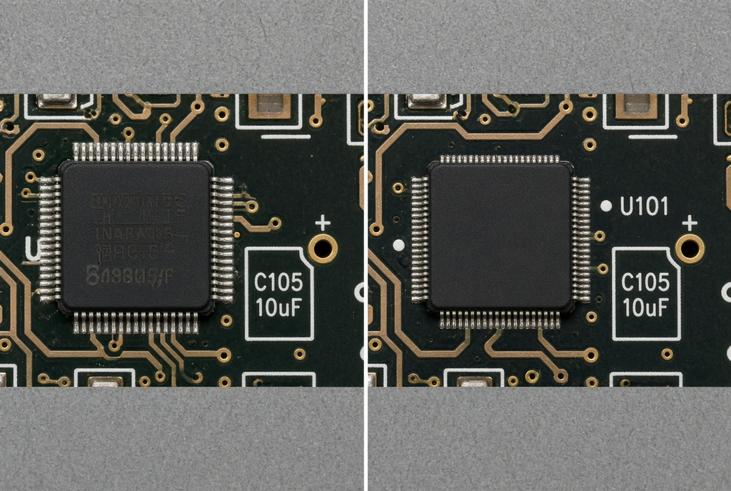
Reference designators hidden by components
In an empty layout, it looks neat to have parking U12 directly under a 15 mm inductor, or squeeze C3 into the courtyard of a large electrolytic. After assembly the designator is gone. First article inspection is then based on counting pins from a corner. Rework is reliant on the technician removing the assembly drawing and hoping that the board revision matches.
Position all designators so that they will be visible after soldering the package. A short leader, or a consistent offset direction (all the designators above and to the left, for instance) is easier to learn than a random scatter of designators on a dense board. Do not stack two designators – if they overlapped move one.
Missing or ambiguous polarity and pin-1 marks
Diodes and tantalums can be reversed and connectors can be placed 180° off due to the absence of polarity marks on a silkscreen. It’s almost as bad if the marks are ambiguous: a tiny notch that could be pin 1 or a mold mark, a plus sign in the middle of the body instead of on the positive pad, or a pin-1 dot that’s similar to a via tent.
Use one polarity language on a board and match the family of components. Ensure that the mark indicates the right pad after the footprint was mirrored or reused from another design. A footprint copied from a library where one of the pin-1 corners is assumed to be different will print a confident incorrect footprint.
Decorative text, logos, and non-essential graphics
The functional legend gets all the available space of the open mask available from large logos, strings of slogans, and ornamental borders. They also strike test points, mounting holes and keep-outs. You can have branding on a board. When it is used in competition with a designator, polarity mark or revision, it should lose the argument.
For the marketing, if they desire a mark, put it on an unused part of the panel rail or a non-critical corner of the panel rail after the functional list is installed. Be careful not to have a logo cut into a test pad or cover pin 1 of the main connector.
A Pre-Release Checklist for PCB Silkscreen
Treat the legend layer as a Manufacturing Document, not as “leftover annotation” before you export Gerbers. The defects listed below won’t be detected by DRC (electrical).
Functional legend priorities
Include at least:
- A name for each component placed, which must be located by the assembler and inspector.
- Polarity marks on each polarized part.
- Polarized headers and connectors with pin-1 indicators
- Test-point labels with the name of pads adjacent to them.
- Label board part number and revision where it won’t get damaged at assembly and depaneling time.
If the board is too full for all of the graphics, start cutting graphics, then descriptive text, then secondary logos. Do not cut polarity on parts which fail when reversed.
DFM and clearance checks
Test the Legend against the copper, mask, drill and the 3D component step models:
- No exposed silkscreen on pads, test points or on exposed vias used for probing.
- Edge, slot and mechanical keep-out clearance to prevent routing and handling from erasing marks
- The height and width of the text to be formed within the fabricator’s process window for that construction
- Designators that can be seen after parts are installed, such as tall parts, connectors and shields
- Polarity & pin-1, uniform throughout.
- Graphics that do not support the function removed or moved from non-functional areas.
The size of a string must be correct, if it can only be fitted by sitting on a pad, then it must be a different string or the placement must be different—don’t just send a request to the fabricator to “print around the pad.”
Frequently Asked Questions
What is the purpose of PCB silkscreen in manufacturing?
The human readable information that assembly, inspection, test and field service require on the physical board is on PCB silkscreen: reference designators, polarity and pin-1 marks, test labels, part number and revision. Does not have current, nor does it define solderable openings.
Should silkscreen be placed on pads or test points?
No. Ink on pads is detrimental to inspection and solderability. Probe contact is interfered by ink on test points. Do not place the PCB legend layer over any solderable and/or test surface, even if it involves moving or shrinking a designator.
What information is essential to include in the silkscreen layer?
The minimum: Parts identifier indicators, polarity markings for polarized parts, pin-1 markings for ICs and connectors, Testpoint labels and a visible board revision and part number. Decorative marks are last on the list.
How can I make sure reference designators are visible after assembly?
Do not place any designator outside the completed body of the component, but also outside the space used in the courtyard. Look at the 3D view or a first article picture taken at a regular bench angle. Avoid using offset strings to the left of tall parts, connectors, or shields.
What are the most common silkscreen mistakes in PCB design?
Hidden designators, missing or inconsistent polarity and pin 1 marks, legend printed on pads or test points, too small text to read after print and assembly, and logos which take up the space taken up by the functional marks.
Does silkscreen affect electrical performance or only assembly and service?
The property of the silkscreen ink being non-conductive does not constitute a property of the electrical. It is involved in assembling, testing and servicing. The electrical risk is only indirect: Ink on a pad or test point will affect soldering or probing, and a misplaced polarity mark will cause a part to be inserted upside down.