What is an LED PCB? It is a printed circuit board that is designed to conduct electric current to LEDs and, importantly, to remove heat from the LED junction into the PCB and finally to a heat sink or enclosure. Weight, choice of dielectrics and thermal vias are not finishing details. They are the way that junction temperature ensures that it remains within datasheet limits and light output doesn’t roll off after a few hours on the bench.
This is not a standard FR-4 logic board with LED footprints. This stack-up can power a microcontroller for years and a high-power array and the majority of the heat escapes not through the air, but through the bottom of the package. Metals core lamps or other heat optimized lights are commonly used in lighting boards. If you have a project requiring that type of board for your LED project, you can begin with an aluminum PCB.
How an LED PCB Differs from a Standard Board
To understand what an LED PCB is, consider two of the constraints that a logic board does not usually have to deal with: a) current per string, and b) heat under the pad. For a high power array, the packages are placed on large thermal pads, the copper plate is thick and the substrate selected to have a high thermal conductivity to the copper plate or package housing. The same number of LEDs is used with the same number of packages and all of the packages are mounted on small pads, the copper is sized for signals and hot spots are seen as discoloration or early dimming on a thin FR-4 strip with the same number of LEDs.
The board is still a circuit. There’s still a bit of traces, pads and solder mask. The difference is that electrical routing is just 50% of the work done. The other half is a continuous thermal path connecting the semiconductor junction with the room.
Current and copper requirements
The amount of current carried in a LED string is typically much greater than a GPIO or a sensor net. Hundreds of milliamps can be taken from a single high power emitter. Those currents on the common returns can be added together in a series-parallel array. The same geometry is used for a 20 mA indicator and is a resistive heater if used with a lighting string.
The voltage drop is similar in shape. The first LED in a string is connected to a long narrow trace that drops the voltage so the final LED doesn’t get it. Brightness becomes uneven. Local heating is counter-clockwise around a low-level high-pressure center. Typically, it is a layout habit from the digital boards; 0.5 oz copper and traces sized for signals, then a first article that is running warm along the power path.
The wider the traces and the thicker the copper, the lower that resistance is. They also distribute heat outwards rather than in one pad. The amount of copper required is dependent on the current, the trace length and the amount of heat the copper is to carry, or not, out of the air. It’s a design decision and not a standard value.
Heat concentration under the LED
The majority of the heat from a power LED dissipates through the thermal pad on the base of the power LED. The datasheet junction-to-board or datasheet junction-to-case figure assumes the pad is soldered to copper which will tolerate the heat. Use the same setting as a small indicator and a small pad, few signal vias and a CAD-appealing mask opening will be drawn. When the junction is on the bench, the heat is not able to flow away and this is why the junction rises.
The board must be able to endure the heat, and transfer it. In a metal-core construction, the path would be: pad, dielectric, metal base, heat sink/housing. On FR-4, the path is pad, thermal vias, the other side of the board (inner copper), or whatever is attached to the board. If any link in that chain fails the LED loses that link in temperature.
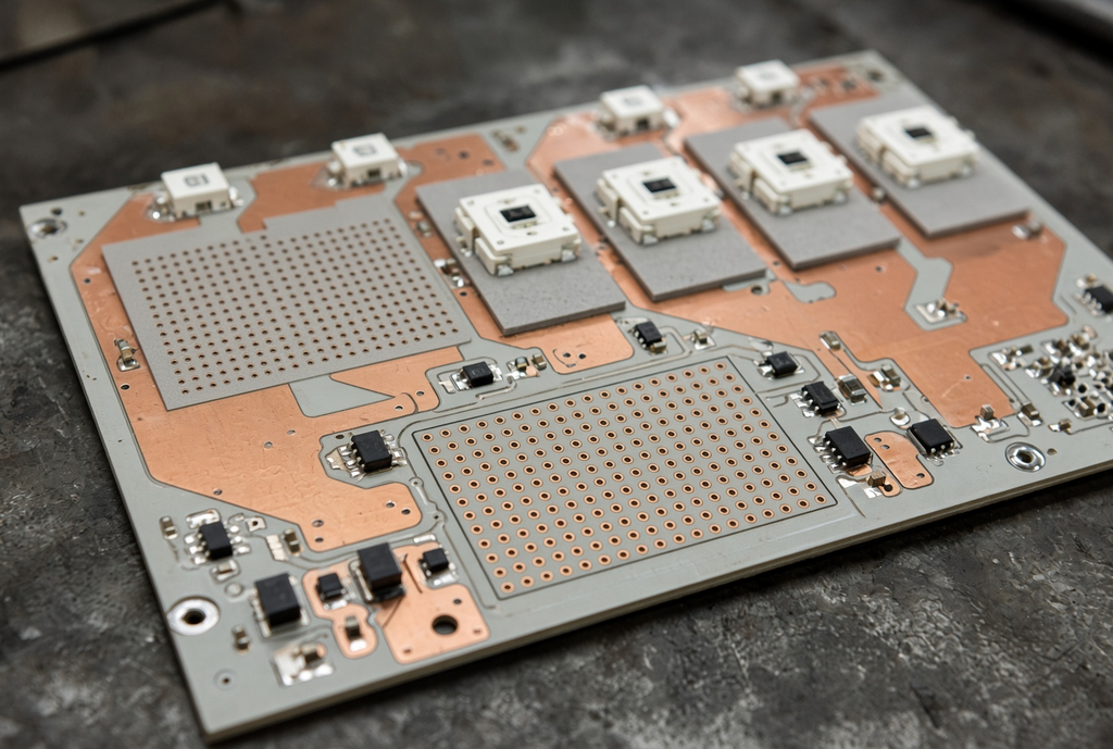
Common Materials for LED PCBs
The selection of materials for LED PCB is not only based on the electrical isolation property, but also has the requirement of thermal conductivity and mechanical fit. The industry options are the families listed below: Availability, thickness in the dielectrics, copper weight, and finish must be verified by the fabricator, and not taken from a catalogue page.
FR-4 with heavy copper
In some cases, lighting boards remain on FR-4. This can be done if the power per LED is moderate, the array is far from each other and the designer is willing to apply actual copper and via patterns under the pads. The heavier the copper, the better it spreads and the better it conducts current. A few isolated pours are aided by a solid copper plane under the array.
A heavy copper is no cure-all solution for missing path to environment. With no airflow, no metal housing and no heat sink, the additional ounces provide time, not a steady junction temperature. FR-4 is also known to have poor through thickness conductivity. If heat has to be transferred from the component side through the laminate, it must pass through vias or it will not transfer.
Metal-core (aluminum and other metals)
The thin dielectric layer is placed between the circuit copper and a metal base (typically aluminum, sometimes copper) in a metal core LED PCB. Thermal highway is the base. When heat enters the dielectric it flows through the metal and into a heat sink, luminaire body or chassis.
The limiting factor is the dielectric. Heat transfer is accomplished by a thin layer of higher conductivity fluid. If there is a thick or poor quality layer, it reduces the cooling property of the metal plate into a heater. Mounting also matters. If the metal-core board is not pressed flat against the heat sink, or if an interface material (thermal glue) is employed with voids, the benefit of the purchase of the substrate is cancelled out.
Metal-core boards are changing the assembly and machining habits. The quality of the routing, V-scoring and quality of the holes are different from FR-4. Thought should be given to fasteners and connectors since the base is conductive. These aren’t questions that need to be asked after the first warp, they are questions that need to be asked before the first panel.
Ceramic and other high-thermal substrates
Very high power modules and designs requiring a stable thermal path in a severe environment will use ceramic and other high-thermal substrates. They can withstand high heat flux and can maintain good dimensional stability. They’re also more expensive, can be harder to assemble and may require assembly processes not being performed daily by a standard SMT line.
A popular “surprise” is the choice of an exotic substrate due to its appearance on the thermal plot. Look at the cost, size of the panels, the process used to get to the via, the surface finish and if the assembler can reflow that board without a special fixture. The exotic option is not required, it’s just an option if the metal-core/heavy-copper FR-4 stack-up is already providing the junction temp cooling within the limits with margin.
Thermal-Design Basics for LED Boards
LED boards thermal design is a path problem. Heat begins at the connection, flows into the package, then through copper and vias or through a dielectric into a metal base, and then out through a heat sink or the air. Thermal resistance exists for each interface.
Junction temperature and why it matters
The Life time and the lumen maintenance of LED are dependent on Junction temperature. A maximum and often derating curve are found in datasheets. The higher the junction, the less light is emitted. Color can shift. Bright design at switch on, weak design after 20 minutes is a thermal-path issue, not a driver issue.
Designing for ambient temperature is not the objective; rather it should be the starting point. Most first articles fail when they go from ambient to board, and from board to junction. The 25 °C lab is not the same product as a 50 °C fixture cavity. Design for the duty cycle and cavity you will be shipping.
Thermal vias and pad design
Typically, a matrix of thermal vias goes through the LED pad to either draw heat into inner copper or to the other side or into a metal core. The vias should be placed in the heat path, so under the thermal pad, not in a circle one millimeter away and the pad seems crowded.
Some small off-center vias will not dump what the package is dumping. The amount of heat conducted depends on the diameter, number of counts and thickness of the plating. Filled or capped vias can enhance the solder interface and minimize voiding. The effect of tented vias on solder behaviour during assembly. These are suggestions to consider with fabrication and assembly, NOT rules to be followed on an unrelated board.
The pad itself should be the same size as the LED, with the thermal pad, and should leave a solderable area that can be wet and won’t cause the package to “tombstone. Copper with a bigger size around the pad aids spreading. Soldermask defined and copper defined pads are different aspects of solder volume. Choose one of them with the assembler, then make sure it is the same throughout the array.
Copper weight, planes, and heat spreading
Large copper and separate thermal planes distribute heat laterally rather than having to exit from the board. A continuous pour under an array is similar to a heat spreader. A pour that narrows to a thin neck does not. Gaps in the isolation may be cut to open the way for wiring and result in multiple islands.
A signal board will require less copper than a high current lighting layout. If the current and thermal load are too high for standard copper to be able to support cleanly, then it is a conversation that needs to be had before the stack-up is finalized: what is a heavy copper PCB for high current LED boards? These are also influenced by heavier copper. These restrictions should be in the design rules, not as an add-on on the gerber.
Stack-Up and Layout Considerations for LED PCBs
The thermal path is converted to copper and layers a fabricator can build with LED stack up and layout. Questions have to be practical: where does the heat go into the board, which layers do it use, and how does current go to each string without heating the wrong neighborhood.
Layer count and thermal layers
You can still use almost all of the “2-layer” LED board as a thermal plane. Multilayer boards could be used to spread in the inner layers and strings and connectors in the outer layers. A 4-layer board of lights will end up having 4 layers of routing and no thermal plane, unless layers are counted only when routing.
More commonly, the metal components are single-sided on the circuit face, where the metal base provides the spreading. The process of adding a second circuit layer to metal-core is different from that of adding a second layer to FR-4. Never assume a standard multilayer stack-up without the fabricator’s consent that it is being constructed.
Component placement and current paths
Install LEDs for heat to dissipate. A very common first article complaint is clustering a high-power array in one corner and the nearby parts just don’t live. Do not overcrowd the plants. Put the driver and sense parts where they see a cooler region of the board.
Make high current circuits short. Long outbound and return paths bring voltage drop and heat radiation along the traces. Connectors to feed the array should be placed where the copper can be made thick rather than at the end of a skinny neck. When it comes to using a metal housing as a heat sink, design the holes in the layout and the thermal interface before the layout is fixed in place.
Solder mask, finish, and assembly
Both solder joint and thermal interface pad is influenced by solder mask and the surface finish. A mask that is raised over the thermal pad decreases solder area. The colour may not be suitable for the reflow profile or the shelf life required by the assembler if the colour is being selected for a visible board.
Building on metal-core isn’t the same as building on FR-4. Heat absorption by the metal base requires an adjustment of reflow profiles. The change in warpage, fixture support, and depanelling of the panel all vary. Be sure to mention those items in the assembly package. With a Guangdong PCB and PCBA partner like CKS Circuits, you can check the PCB and PCB assembly data before production to ensure that these mismatches are identified in the form of questions and not as a pile of LED’s that have been ‘tombstoned’.
Common Applications for LED PCBs
The common problem on the LED PCB is that the current and heat are concentrated into a small area; there is a path to a housing and a strip. The optical and mechanical design of the luminaire is beyond the scope of this article. This product still needs to pass the heat and electrical load of the board.
General lighting and luminaires
In the case of indoor downlights, linear fixtures, outdoor heads etc., the housing is the heat sink, and as such, metal-core or heavy-copper boards are generally used. The board provides a connection between the LED pads and that housing. Common field problem: Thin FR-4 coupon in sealed outdoor fixture; cavity is hot, dielectric is thick and there is no air to help.
Not all general-lighting boards are high-power. Low power runs (decorative) should be on FR-4 provided the copper and via pattern are truthful about the load. The error is assuming that all general lighting is a low power product due to its recognizable product category.
Displays, backlighting, and signage
Strips and modules that are used for displays, backlighting and signage are not as concerned about peak brightness as they are about uniformity. Thermal roll-off after warm up will appear as a darker area in the middle and/or a color change down the strip. That’s worse when there’s thin copper and long strings. If you see hot spots on your mask, that is a layout warning, NOT a cosmetic problem.
These products will also penalize voltage loss. The customers always see the LED of the end of the long strip first. The size of the copper should be for the string current, not for a six” piece on the lab bench.
Automotive, industrial, and specialty lighting
Automotive, industrial and specialty light come with added vibration, extremes and extended life. The materials and finishes of the board must be rated at the same level. Starting with a lighting stack-up for a consumer or dropping it into an engine bay or washdown fixture is the wrong approach.
A decorative strip doesn’t need to document, trace or cover all of those markets. Consider those as project requirements. They do not mean that just because the board has LEDs on it, it is implied that every fabricator is qualified for every regulated use, nor do they mean that every fabricator is qualified for every use.
Common Mistakes in LED PCB Design
The following failures pop up on first articles more frequently than exotic material debates. These are all short circuits or broken voltage/short circuits in the circuit that appeared to be OK in the CAD window.
Undersizing the thermal path
Field stories on too thin copper, too few vias under the pad, or a poor dielectric on a metal-core board are alike in that the LED runs hot, output decreases, and life is shorter than what was promised in the datasheet. The package is obeying the laws of physics. The heat was not taken by the board.
Adjust the path first, then the LED. Even if a higher-efficacy emitter is on the same broken path, it will still dump heat into a small pad.
Ignoring current density and voltage drop
The long thin traces on a multi-LED string present two issues. The brightness is not uniform throughout the run because of a voltage drop. The same traces heat locally, thus increasing the local board temperature and providing the first problem. For the first article measure the voltage at both ends of the string. If the last LED is dim, then the copper is “talking.
Treating the LED as a simple indicator
The power LEDs arranged in a 0603 format are easily visually identified because they have very small pads, no thermal via field, mask that is pulled tight and a comment that this is “only an LED.” It isn’t just an LED! Thermal pad is a heat port. If its that port is on a signal sized pad, the connection will rise until one thing gives way, either solder, phosphor or the customer’s lumen spec. gives—solder, phosphor, or the customer’s lumen spec.
A Simple LED PCB Design Checklist
Answer these before the stack-up and layout are treated as finished.
- Answer these questions prior to the stack-up and layout being considered complete.
- What is the power per LED and the junction-temperature target at the real ambient (not at the lab bench)?
- On which substrate family is the thermal path constructed: FR-4 with a predetermined via pattern, metal core with a specified dielectric material or a special high thermal substrate?
- What are the copper weight and strategy of the planes, and where do the planes narrow?
- How many thermal vias are located below each LED thermal pad and do they connect to copper that extends on?
- Does the board have a direct path to heat sink/housing or other heat interface, flatness and mounting?
- Are high current loops kept short and do hot packages keep away from sensitive parts?
- Are solder mask, surface finish and assembly notes consistent with the pad design and substrate (solder metal core or depaneling constraints)?
If any of the above answers remain “we will see on the first article”, the board cannot be quoted as a lighting PCB. Close the thermal path similarly to the schematic netlist.