Copper-clad laminates are the layup used for almost all rigid and flex PCBs; sheets that have copper foil on one side, and a resin-reinforced dielectric on the other. This sheet is generally used by the designer as a “black box”: “thickness” and “copper weight” – and nothing more. The type of the resin system, reinforcement and foil type are still important to consider for the etching of traces, reflow of impedance, lamination of the stack, and passing thermal cycle of the vias and copper.
CCLs of the same thickness and copper content do not have to be made interchangeable. The nominal construction of a standard epoxy core, a high Tg multilayer construction, a low loss high frequency sheet and a polyimide flex CCL can be different in the case of various etching, warping and aging. It is important to know what makes up the CCL so that you can ask the right questions of the fabricator before locking the stack-up.
Basic Structure of Copper-Clad Laminates
A copper-clad laminate is NOT “a board waiting to be etched. Basically, it is composed of three parts which are later on converted to cores and combined with prepreg to form multilayer stackups. You only have described the envelope, not the material, if you give only the finished thickness and copper weight. The combination of foil-resin-reinforcement is the CCL structure used in PCB work, and it is used all throughout the etching, laminating, assembly and field life processes.
Copper Foil: The Conductor Layer
The material that will be the traces, planes and pads is the copper foil. Only two families seem to be commonly used in PCB programs.Two families are brought to the fore in PCB programs.
For the electrodeposition (ED) of copper, a drum is used. It is relatively isotropic for grain and is popular for use in the rigid boards by fabricators because of its predictable etching pattern for common line & space rules. Mechanically reduced and subsequently annealed copper is called rolled annealed (RA) copper. The grains are elongated in the direction of the rolling which provides for better flexibility and fatigue life in the case when the copper is used for bending. That’s why RA foil is the most common ‘beginning and end’ material for flex circuits and certain forms of flex construction that require a large number of flexes to be created and bent many times over a period of years.
Both types of foil are “good” in and of themselves. This should not be confused with ED copper on a rigid digital board and RA copper on a flexible dynamic tail. These three functions are lumped together in grain structure, foil treatment and the etch by the fabricator. A way to bend
Resin System and Reinforcement: The Dielectric Backbone
Dielectric is the resin and the resin carrier, the reinforcement. Most of the thermal and electrical properties are in the form of resin – epoxy for general purpose boards, higher Tg epoxy for more reflow or higher operating temp range, low loss where high impact on signal integrity is required, polyimide for flex or high temp stability. Reinforcement controls how the sheet handles, how the sheet is laminated and the dimensionality of the sheet in heat, with most rigid boards made up of a woven sheet of glass and some flex and specialty constructions being different fabrics or non-woven systems.
Resin content is not a footnote nor is the glass style. They change the coefficient of thermal expansion, glass transition properties and the dielectrics constant and losses the plated via is subjected to. With the same finished thickness, but a different resin and a different glass, the finished piece will look “cleaner” when electrically evaluated and will press the same in different ways. So, if you select the same actual CCL family, two drawings with the same “1.6 mm, 1 oz” specification can yield different impedance and warpage.
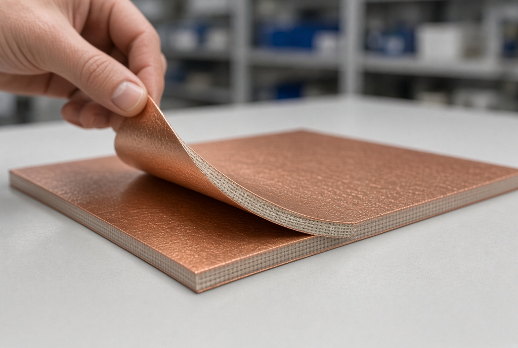
Types of Copper-Clad Laminates by Resin and Performance Class
This is best done when selecting types of copper clad laminate, as starting with the job the board has to perform, rather than by starting from a catalog name. The families listed below are performance classes. Obviously the fabricator will have more than one qualified sheet in each class and the “right” sheet is not necessarily the number one search hit, but rather the one that fits the electrical, thermal and process window.
Standard Epoxy and High-Tg CCL for General-Purpose and Demanding Boards
Most digital, industrial-control and power boards are made from standard epoxy CCL. It is commonly used by most shops, can be used on well-known processes and is the default option when the design is not based on frequency, loss or extreme temperature.
High-Tg CCL is not a material, but a class. Use the board when there is a thicker multilayer stack, or a higher operating temperature than a standard epoxy can operate at, if the board is to be used during a lot of reflow cycles. The typical reason for the use of “high-Tg” is that it will not melt during lamination and assembly, but not necessarily because it will have better electrical numbers. Ask the fabricator which ones he/she has already processed that have a high Tg; don’t lock one from a datasheet that he/she has not already processed.
Low-Loss and High-Frequency CCL for RF and High-Speed Designs
CCL with low loss are for high frequency applications where controlled-dielectric-constant, low dissipation factor and frequency/temperature stability are required. It is the home of RF front-ends, microwave circuits and high-speed digital links, where the loss and tolerance of impedance become “close enough” issues.
They are usually higher priced and require more etching control, more attention to roughening the surface of the foil and notes that are consistent with the material family. Low loss CCLs are a key specification and need to be considered during panelization and during a program’s impedance modelling as an FR-4 commodity, otherwise, the program risk losing money and margin.
Polyimide and Flex CCL for Bending and High-Temperature Applications
Polyimide flex CCL is NOT thin FR-4. When using flexible or rigid-flex circuits, a different resin and reinforcement system will be necessary because the copper and dielectric must be able to withstand bending, tight fold radius or a hotter environment than a rigid epoxy stack can be designed to handle. In that construction the design rules are different: Coverlay in many places (no solder mask), different via strategies, choice of foil depending on the bending requirement.
If you need a flex tail (or if a 3D fold is necessary for a small enclosure), start the conversation with a flex construction. The “make FR-4 thinner” until it bends is a late stage redesign that’s ready to go.
Copper Foil Types and Their Impact on Etching and Reliability
Copper weight is just one of the variables of foil. The type, treatment and surface roughness influence the etching process and the copper after the board is built. Those details can be seen as yield and field reliability and not as a line on the quotation – when it comes to fine-line rigid work and flex.
Electrodeposited (ED) Copper vs Rolled Annealed (RA) Copper
The decision of whether to use ED vs RA copper foil PCB should be based on the mechanical, etch job, and not on habit. Although not as common as in the past, most rigid boards are still etched with ED copper since the shops are accustomed to the etch properties of the copper and the part is not intended to flex. It is desirable to use RA copper in repeated bending applications, or when fatigue life is a component of reliability case, due to its elongated grain.
Either a rigid multilayer, or a flex circuit, with both using standard ED foil and RA foil respectively, may be “1 oz copper” on paper. They do not replace each other. If the design is fixed at the beginning and extended later, it is important to check the foil call out, as with the bend radius.
Foil Treatment, Roughness, and Signal Loss Considerations
The resin is coated with foils so that it will adhere. Such treatment usually leaves a certain texture. This is an adhesion and etch factor, mostly at lower frequencies. At high frequencies, it’s a loss story—a rougher interface of the copper-resin can lead to a longer path and lead to higher insertion loss. The very smooth foil could be used for electrical numbers and a special treatment package is needed to ensure that foil does not lift during processing.
If loss budgets or fine-line etching is limited, include foil type and surface condition with dielectric class. The fabricator can then state if the requested foil is something that they are able to run in the machine or if there is a smoother or treated foil that will still meet the adhesion and electrical target.
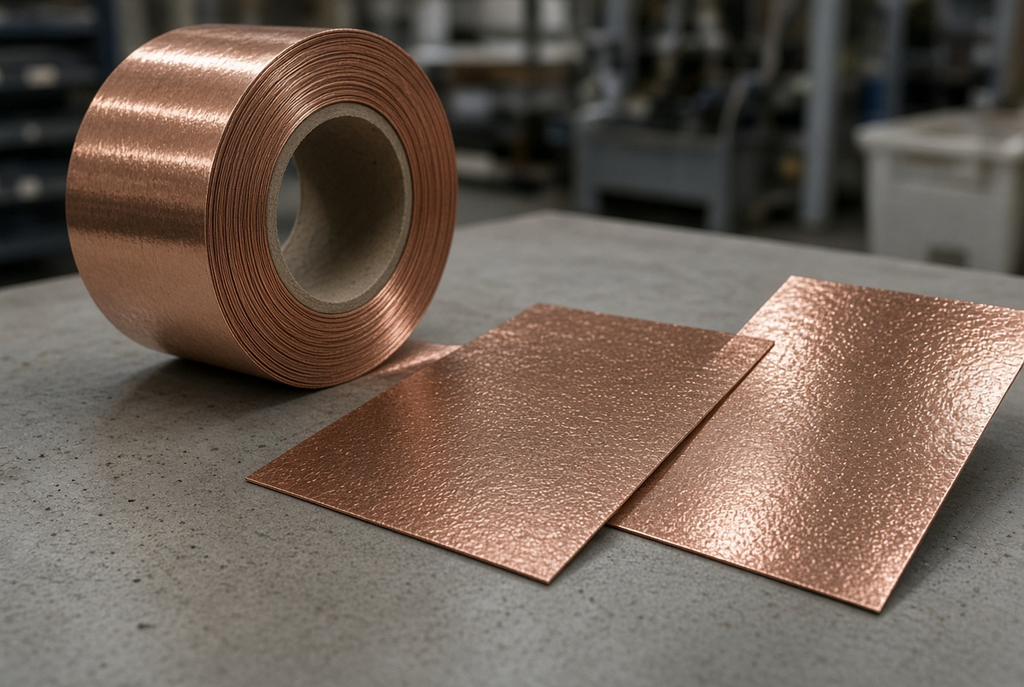
How CCL Becomes Cores, Prepregs, and Multilayer Stack-Ups
Upon entering the press, you’ll have a better idea of the role that CCL plays in PCB fabrication. The last dimension of laminate is not the thickness of the board. It’s where cores are made, cores into the stack, and the rest of the stack gets its magic properties out of.It’s the source of cores, and the cores and prepreg make up the stack, which acquires magic properties from the rest of the stack.
From CCL Sheet to Core and Prepreg
Core consists of a copper-dielectric-copper structure that is cut to the appropriate thickness and copper thickness by CCL. Prepreg is the partially cured resin and reinforcement materials that are used to bond cores. These cores are separated by the prepreg after being laminated.
The previous CCL properties remain at this stage. Resin system and glass style, resin content and foil type are kept within the completed multi-layer. Although a stack may be correct in a layer-count drawing, it can still not satisfy the impedance requirements or warp in the press when the thickness is wrong and the wrong core and prepreg family is selected.
Why Stack-Up Designers Care About CCL Properties
The “how many layers and how thick” is just a portion of the solution to the stack-up and signal-integrity problem. The rest of the sentence is on the effect on impedance and reliability of implementing CCL. The effects of the dielectric class and resin content shift the effective dielectric constant. Roughness and loss tangent of the foil is responsible for the insertion loss. With plated-hole stress, the mismatch in CTE between the copper, the resin and the glass is observed. The thickness control after press (impedance scatter) is represented by resin flow and glass style.
A good stack up note should NOT only be a thickness or the final thickness, but also the class of material and the use of the foil. This is the difference between a drawing that a fabricator can create and a drawing that will be modified after the first impedance coupon.
Common Pitfalls When Specifying or Selecting CCL
The exotic chemistry failures are not most of the CCL problems on a program. Spec habits – treating the sheet as a commodity, ignoring the foil or when a flex has been locked and the shop has not been successful with it.
Treating All CCLs as Interchangeable Commodity Sheets
The general guideline is “the same thickness copper as the original and cheapest available.” The teams will be subjected to impedances that will change when they change the material, extra loss caused by a high-speed pair, warpage after lamination and stress resulting from the thermal cycling. The drawing wasn’t concerned with resin type or foil type, and hence, the choice of these variables was optimized during the buy.
Alternate – two CCLs may be used as an alternate; must be alternates within the same performance class and must have the same intent for foil and dielectric properties. Only cost is involved in equivalent swaps, not class.
Ignoring Foil Type in Flex or High-Reliability Designs
The normal ED copper flex circuit is a bet you didn’t want to be placing. The trace may appear flawless after etching, and the bend may not work out after the process. When the foil roughness isn’t accounted for, the same class of miss comes up on the high frequency boards, the stack is still ok, the lines are still ok, and the loss is still worse than the model since the copper-resin interface wasn’t part of the model.
For copper which requires flexibility, fatigue life requirement, and tight loss budget with rough surface, use foil type.
Locking a Material Without Checking Fabrication Experience
Process windows do not move as fast as datasheets. While looking online for a CCL grade, the team writes the part number down on the fabrication note only to discover that the qualified list or compensation or the press cycle around a different family in the same grade appears. This leads to an article change late, an article re-quote or a first article that fails to match the article model.
Tell the performance requirement (frequency, loss, temperature range, profile, bend or stiffness limits), and allow the fabricator to suggest CCL families that they are familiar with. Electrical and Mechanical targets will continue to be owned by the same as before. It’s up to them whether those targets will be on a given sheet or not.
Practical Guidance for Working With Your Fabricator on CCL
The helpful talk is concise and to the point. Use your own judgement on the application requirements. The store gives the items that it can actually operate.
Start From Performance Requirements, Not Part Numbers
Describe to the board what it must withstand, and how it must function: operating frequency, loss budget, impedance tolerance, maximum assembly temp and number of reflows, operating temp, rigidity/bend life, and any environment that poses a stress to plated vias. Doing the same as another project’s part number is a guess, not a must. If qualified the fabricator may certify this grade. Otherwise, they will stay in the same class and wouldn’t need to redesign around an unavailable sheet.
Use the Fabricator’s Qualified Material List as a Starting Point
Most fabricators have a database of CCLs that they have been etching, laminating, and have the reliability data for. List that is used as the menu. After determining which families make for acceptable options, further restrict to performance, cost and schedule. It might be worthwhile to request a shop to test a new CCL on one prototype. It will not be added as a default if a class has been added to the qualified list as well.
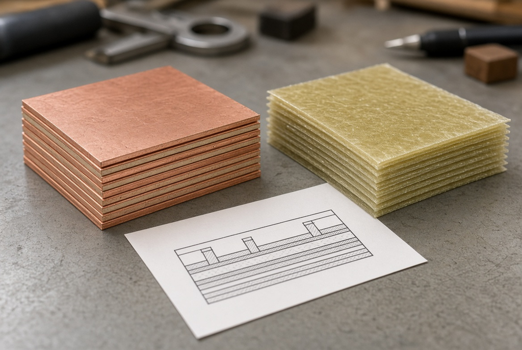
Summary Guidance – Treat CCL as a Design Input, Not a Black Box
Copper-clad laminates are not necessarily and only found in the PCB warehouse—these are design inputs. From the incoming sheet to etch quality, reinforcement and foil type to impedance, thermal behavior and via reliability. Consider those three parts a foregone conclusion like layer count and copper weight.
Explain the performance concern that you want to address, but in materials that the fabricator is familiar with and in which he or she is familiar with producing the class/fabric, not the thickness and ounces. This is how CCL becomes a tool to be managed, rather than a black box.