Surface finish types for PCBs are protective coatings which are applied to all such exposed copper areas to prevent the surface oxidation of the copper before assembly and to allow the wetting of a clean surface with solder. The finish of the fabrication drawing is not a decorative spec line. It affects the amount of wetting of the paste, the flatness of the pads for fine pitch/BGA components, the storage solderability of the boards, and the inspection of the assembly line. The “best” finish is not a single one, but rather a set of them. ENIG is not an automatic improvement over HASL and an OSP board can be prepared cleanly during handling and storage and with the same coating during reflow. The best choice is the best design for the components, thermal process, storage plan and contacts for that particular design.
What PCB Surface Finish Actually Does
The copper surface which is to be soldered is exposed after etching. The copper can oxidize, get fingerprints or foul residue between the end of the fabricator’s wet process and the first application of the paste. Until soldering, the coating on the surface is the substitute for that copper. Even if pad design and stencil design are right, the solderability degrades once the finish is affected by oxidation, contamination, or scratching. One of the quickest ways to purchase opens and weak joints is to assume anything will “just work” after several weeks of open air handling.
Protecting copper and enabling solder joints
The practical jobs are easy. The finish protects the copper from exposure to oxygen and contamination until heat and flux take their action. It also provides a surface to which molten solder can wet. The different finishes do those things with different metals or organic films, hence their different aging and different looks when viewed under a microscope. The reason for the finish being a part of the manufacturing data package is that it is a process input and you do not choose it after the boards arrive in your catalog.
Influence on assembly process and inspection
In the line, finish is manifested as wetting, self-alignment, and inspection noise. When there is uneven or inadequate wetting of a pad, the paste may form an open joint, a starved joint, or a non-tombstoned area. This is a harsh spot for fine pitch and BGA packages as there is limited volume of paste available to lose in a high or oxidized pad. AOI and visual finish also read finish. Stained OSP, tarnished or uneven HASL can cause false calls, or it can mask a true fault that is adjacent to a noisy pad. Aside from the bare-board photo, a PCB finish for assembly must pass print and reflow and pass inspection.
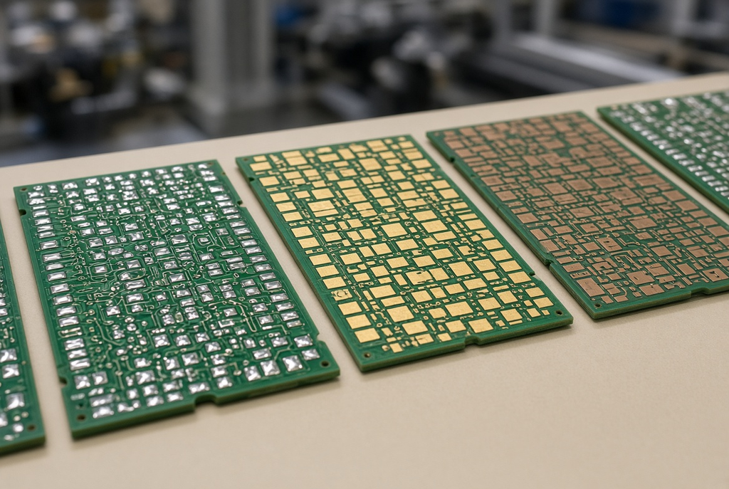
Common PCB Surface Finish Types and Their Characteristics
There is no need for a “lecture in electrochemistry” for designers and buyers. They should be able to tell where each family is generally used, its merits, and its drawbacks. The notes below describe industry practice, and do not guarantee that every fabricator or construction has every finish available on every stack-up.
HASL and lead-free HASL
Hot air solder leveling applies molten solder to the exposed copper surface, and then uses an air knife to remove the excess solder. In the past, the traditional HASL was a tin-lead alloy. Instead, the tin-based alloy is used in the production of HASL (tin) PCBs, and is the type that most lead-free programs are expecting. Both provide good initial solderability and they are frequently a lower cost option for designs with a coarser pitch. The compromise is the surface topography. A soldered finish is not so planar as a plated or organic finish, as the solder tends to crown or thin at the edges of the pad. This unevenness is fine for many through-hole and larger pitch SMT components. It becomes a problem when the finest device on the board requires a flat surface to land on to adjust paste volume and to self-alignment. Not all fabricators are still using both leaded and lead-free HASL – specify the family of alloys used in the work process.
ENIG (Electroless Nickel Immersion Gold)
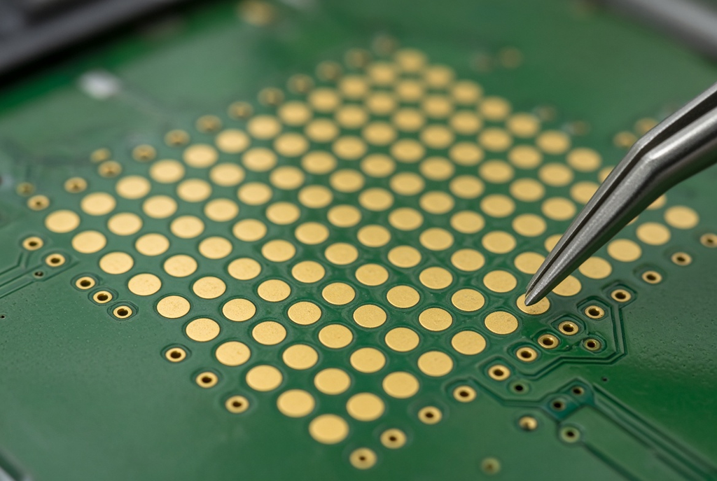
ENIG is a nickel barrier with a thin gold flash. The gold prevents the nickel from oxidizing; during soldering the gold volatilizes into the solder and the solder wets the nickel. The surface remains flat, that’s why it is considered one of the most popular comparisons for fine-pitch or BGA boards: ENIG vs HASL. Generally, shelf life is less critical than the thin organic coatings when boards are packed and stored in a reasonable manner. More expensive than HASL or OSP and requires control process. An interface that is brittle, sometimes referred to as black pad, is a consequence of poor nickel and/or immersion-gold chemistry. This risk is controlled through process control and incoming inspection, rather than as a universal upgrade of the ENIG. Use it when there is justification for use for flatness, mixed assembly, longer storage, etc. – not just because a previous project used it.
OSP (Organic Solderability Preservative)
For making PCBs, OSP finish is applied in the form of a thin organic film to a clean copper. Very flat, and typically low cost, coating. When reflowing for the first time, the flux will peel the film, and solder will wet the copper. The strength is weakness. A metallic finish is more effective than handling, humidity and additional thermal cycles. Boards that will be stored in a warehouse, move between several sites, or have multiple reflows and rework require a storage and handling plan similar to OSP or a different finish. A common cause of oxidized pads which appear to be okay until they are not wet by the paste is the use of OSP on a design that needs months before it is assembled, without dry packaging and FIFO discipline.
Immersion silver and immersion tin
The immersion silver PCB finishes and immersion tin are thin metallic layers which remain flattened. They are identified by teams when they want planarity and do not want to use ENIG, or when a contact or assembly process favors that type of metal. Both require process discipline and process discipline in storage. Silver may tarnish in the presence of sulphur or inadequate packaging. On some constructions, tin can cause whisker problems and if the boards remain in storage longer than necessary, they could age in such a way that the ability to solder on the board is altered. Both are no replacement for HASL or ENIG. Outline any special handling instructions assembler needs to follow and document packaging and storage specifications when called out.
Selective gold and hard gold for contacts
Certain areas, such as edge connectors, gold fingers, test pads, and areas that have high wear require a harder, thicker gold than the flash of the ENIG. The finish is generally only used in the area where the contact resides. The remainder of the board retains the solderable finish, such as HASL, ENIG, OSP or other. Fabrication drawing must indicate the boundary clearly, where parts are hard or selective gold, and the boundary between different parts. When the general board finish will withstand repeated mating or probe contact is a surprise at the end stage. Contact requirements are not part of an email after first articles fail at the connector, but should be in the fabrication package.
How to Choose a Surface Finish for Your Design and Assembly
The first thing to consider when choosing a surface finish when designing a PCB is the board you are going to actually build: the finest pitch, package types, how many times the board will be exposed to heat, how long will the board be sitting for, and if there is a wear contact on the board. Those constraints are followed by price and habit, not preceded by them.
Component pitch, BGA, and surface flatness
Fine pitch ICs and BGAs require a planar pad. Paste volume is low, stand-off is close, package needs surface tension to center. The lower the number of high HASL crowns, the less chance of a device tilting or the pads having one side that dries out.The fewer the number of high HASL crowns, the less likelihood of a device tilting or one side of a pad drying. Hence, a PCB finish for BGA work can be considered more of a flatness choice than a chemistry choice. HASL can be used without any drama on coarser pitch SMT and through-hole boards. The problem is: If the previous product was coarse-pitched, and the new product had a 0.4 mm-pitch QFN or a dense BGA, then you may have a problem stating the finish on the previous product, which would be the BGA or QFN package.
Reflow profile, multiple reflows, and process compatibility
Thermal cycles are added by double sided SMT, mixed tech and rework. Some finishes are worse than others for that, as films are consumed, or surface ages between passes. The number of cycles that a particular construction can endure will depend on the laminate, finish, profile and time between operations. No universals exist for reflow-counting rules that can be printed on a drawing. When talking about finish, include the possibility of re-work and/or selective solder and two reflows in the assembly plan. Fine finishes for a single-sided prototype may not be a good choice for a complex mixed-technology build.
Shelf life, storage, and handling
Shelf life is more than just a date on a bag. It is the finish chemistry, packaging, humidity, temperature and frequency of handling the boards. Typically, ENIG ages slower in storage than OSP. It is generally found that the surface should remain clean for good solderability in HASL. Silver that has been immersed must be protected from tarnish. No that will save a board that is left on an open rack next to a fluxing station. Coordinate the actual logistics path with the finish: how much time will elapse from fabricating the board to first printing, for example, and if boards cross-site, and if first-article units are waiting until the firmware or a mechanical piece catches up. As well as the finish name, packaging and FIFO discipline are important.
Connector wear, test points, and special contact requirements
The general solderable finish may not be sufficient if the product incorporates an edge connector, a test interface of type card edge, or pads which will be tested repeatedly. Those features should have a hard gold or other specified contact finish. Test strategy is important. Pads may be damaged by flying-probe/fixture contact on a soft or easily marked finish that will require appearance to be clean at final inspection. The fabrication notes should include a note to call out wear surfaces and probe points so the fabricator doesn’t assume that they are standard SMT surfaces.
Common Surface Finish Mistakes That Hurt Assembly Yield
Exotic chemistry is not the main reason for most yield loss at the end of the production. It is a mismatch of the finish, the parts and calendar and the assembly plan.
Choosing finish based on habit or price alone
The idea of going with “what we always use” or “whatever is cheapest this week” isn’t considering pitch, storage, or reflow. The typical symptoms are seen at first print or first reflow: paste which does not wet or oxidized pads on the boards that lay there for too long, or additional rework on the finest parts while the coarser parts look good. Compare the process of the finish to the process of this design, NOT a template from a less complex board.
Ignoring storage time and handling discipline
Even the best finish won’t be good if the boards are left too long in the boxes, or are handled without gloves or pads. Rusted or dirty pads cause opens and make weak joints that appear as if there is a stencil issue until a person looks at the bare copper. Manage the environment, ensure that moisture barrier packaging is kept closed until print and consider time from fabrication to assembly as a process parameter. When the schedule is missed, check solderability before committing a complete SMT lot.
Not coordinating finish with assembly and test strategy
The problems that can be finished that ignore DFA and test are numerous: HASL on a board with flat BGA pads; no hard gold on a worn edge connector; or finish that results in noisy AOI. Surface finish is an item that should be part of the DFM and DFA discussion along with stencil design, polarity, and test points. Both the assembler and the fabricator will require the same callout with finish, and any selective areas.
A Pre-Release Checklist for Surface Finish
Don’t make finish a “last minute” bullet point on the drawing, it should be a checklist of things to do before releasing Gerbers and the assembly package.
Match finish to components, process, and lifecycle
Verify the smallest component pitch and if BGA and other area-array packages are included. Record the anticipated thermal path: Single reflow, double sided SMT, mixed technology, possible rework. Make estimates for storage time and conditions from fabrication to assembly. Identify the following: List connectors, gold fingers, and high-wear or frequently probed pads. If those answers are in opposite directions (flat pads for a BGA and hard gold on the edge), then record both finishes, rather than one coating to perform a number of different functions.
Confirm finish availability and special requirements with the fabricator
Discuss what finishes the proposed building may be able to withstand. A shop may have certain restrictions because of the amount of stack-up, copper weights, or panel plans that they can process. If you require selective or hard gold, please indicate in a drawing note and on a marked feature list. Use the name the fabricator and assembler use to refer to finish (e.g., lead-free HASL versus a general “solder finish”). The notes may be ambiguous and interpreted on the floor, which may differ from the assembly process you intended.
Frequently Asked Questions
What is the purpose of surface finish on a PCB?
Surface finish ensures that the exposed copper is not oxidized or contaminated when it is fabricated or assembled from the component to the board, and provides a suitable surface for the solder paste and molten solder to form an effective soldered connection. In its absence there is a fast ageing of bare copper and wetting is unpredictable.
Which surface finish is best for fine-pitch and BGA assembly?
There is no best finish in all situations. Generally speaking, flat finishes like ENIG, OSP and most immersion finishes are generally easier to work with for fine-pitch and BGA’s than HASL since there is less pad topography. The more pertinent question would be which flat finish is as good storage time, reflow count, and cost for that program?
How does surface finish affect shelf life and solderability?
Solderability is generally maintained for a longer period of time in metallic finishes than in thin organic finishes, if the packaging is good. OSP and some immersion finishes will be more sensitive to time, humidity and handling. Shelf life is a combination of chemistry, packaging, and calendar; not a characteristic of the finish itself.
Can the same finish be used for all types of boards?
Not reliably. Industrial board, which will be rapidly assembled, can get a different finish to a fine pitch double sided SMT product that will be stored in inventory or have an edge connector. When one finish is used in all designs, it saves a conversation and is likely to be used later in rework.
What are the most common surface finish mistakes in PCB design?
The common mistakes are to select based on habit or price, not considering storage or handling, and leaving contact or test features on the same finish as regular SMT pads. Another common mistake is to call HASL on a board that required a flat pad.
Who should decide the surface finish: designer, assembler, or fabricator?
The callout is the responsibility of the designer on the fabrication drawing, but the decision should be made in collaboration. The designer is familiar with the pitch and contacts. The assembler is well-versed in reflow, handling and inspection. The fabricator is familiar with the finishes that the construction can operate. Boards that aren’t matched up are finished individually by one of those positions.