PCB solder mask is a cured polymer film which covers copper not to be soldered, creates controlled openings over the pads and test points and minimizes solder bridges during assembly. The first thing they notice is color. Most often, opening size, dam width between pads and tenting or leaving vias open will determine whether the board is soldered cleanly or not.
People often mistake mask for a paint job. Masks that are half opened, vias that lose wicking paste and pads that are half covered can not be saved with a distinctive color. This guide is intended for PCB designers, NPI engineers, or hardware teams that must use solder mask as a process layer prior to the sending out of fabrication data.
What PCB Solder Mask Does in Fabrication and Assembly
Solder mask is included in the same data package as copper, drill and surface finish. It’s not something that’s added on the surface of the board once it’s finished. Fabricators image and cure it during the board build. Assemblers, in turn, must deal with the openings, dams and via coverage that this film left behind.
Defining solderable areas and protecting copper
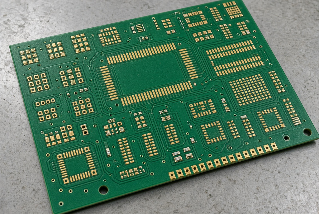
On a completed board, the mask will cover traces, planes and unused copper, which will not be wetted by solder and will have reduced handling, moisture and oxidation exposure. The openings in that film reveal the pads, test points and other features that must be soldered or probed.
These openings serve two functions. They instruct the paste printer and the soldering process where the metal can wet. They also have a wall of polymer between adjacent pads called a mask dam which reduces the chance of molten solder shorting out the pads. Mask minimises bridge risk. Not a substitute for proper pad geometry, stencil design, or reflow control. Boards with poor openings still fail; boards with good openings still fail if there’s a wrong paste volume or profile.
Impact on solder paste, reflow, and inspection
The window the stencil and paste look into is the window openings set. A tight, offset or uneven opening from pad to pad alters the amount of paste receipt at the land, and the amount of spread in reflow. The first to feel it are fine-pitch QFNs and BGAs where the loss of a couple of mils of mask on one side of a pad can cause the joint to be starved or the solder to be pushed towards the next pad.
Inspection takes place in the same geometry. For AOI or visual, the contrast between mask, copper and solder is used to determine the shape of the fillets and bridging. Due to the uneven openings, there are false calls as well as different openings due to process reasons. It’s possible to get the same reference designator to look good on one board and open on the next as the mask registration drifts across a panel.
Common Solder Mask Types and Materials Used in PCBs
A photoimageable liquid system is most commonly used in most production boards. There is a film for specialty constructions that is different in some instances. The polymer recipe is seldom used by designers. They must be aware of family they’re asking for and whether it matches up with family stacking and pitch.
Liquid photoimageable (LPI) solder mask as the mainstream choice
LPI solder mask PCB is begun with a liquid application, which is normally screened or sprayed onto the exterior copper. The film is then dried, then exposed with artwork to create openings, developed and then thermally or UV cured. LPI can use the photographically formed image to resolve small openings and narrow dams required by fine pitch SMT.
That’s why LPI is the default on multilayer rigid boards which go into lead-free reflow. It’s not a one-size-fits-all product. Ink systems vary from vendor to vendor, color to color, gloss to gloss and on heavy copper or tight spacing. Noting “LPI, green” is helpful. It is not a complete process specification, though, if looked at as a whole note. Before you freeze the note, make sure the note is consistent with the fabricator’s standard system with regards to pitch, surface finish and any special via treatment.
Dry film and other specialty masks for specific needs
The dry-film mask is a type of mask that is laminated as a sheet instead of coated as a liquid. It is still used at some fabricators, or a related specialty system, on specific high-density or rigid-flex applications where coating behavior or thickness control is important. There are other specialty films available for special constructions or environments.
The selection of the mask used is usually up to the fabricator after the stack-up and flex regions and minimum features have been determined. A common cause for RFQs bouncing is a CAD specification that describes a brand or chemistry without verifying it is compatible with the specified process. In the case of an unusual construction, state the requirement (resolution, via coverage, flex compatibility) and allow the fabricator to suggest a qualified system.
Solder Mask Color: What It Changes and What It Does Not
The colour of the solder mask on PCB questions is often raised in a new programme. Color is a viable option. It is difficult to say that it is the sole choice that determines yield.
Visibility, inspection, and brand identity
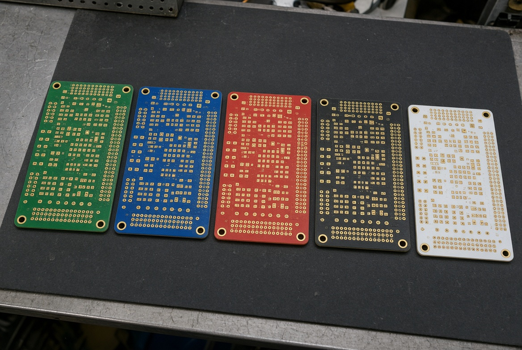
Green is still used because operators and cameras have a long history of contrast habit: copper, solder, and legend all are easily discerned in comparison to a mid-tone green field. The blue and red can be used in a similar way, provided that the legend-ink and lighting match. Black is so striking on a finished product that it can make small cosmetic blemishes stand out; it also absorbs legend, and makes it more difficult to inspect the solder joints when the lighting in the shop is normal. White is suitable for light fittings and some of the consumer fittings, and is easier to show flux residue and handling marks.
That is no justification to ban a color. It’s a good time to choose color when you’re working with the people who will evaluate, modify and service the board, especially with the industrial-design deck.
Color is not a performance specification
Pigment, alone, does not determine the dielectric strength, glass transition or long-term reliability. The reasons are related to the mask chemistry, cure, thickness and adhesion to copper and laminate. The two boards of the same qualified system, but different colored, are significantly closer in performance than two boards that are the same colored, but different in their via treatment or opening size.
Lock openings, dams and via treatment first, when reliability is the constraint. Select color after the rules are settled. A board which looks like the brand and bridges at 0.4 mm pitch is not a branding win.
Solder Mask Design Guidelines for Fine-Pitch and High-Density Boards
Geometric are PCB mask design guidelines which really work in yield. They reside in the relationship among pad size, mask opening, dam width, and via coverage. There are no definitive values for expansion; they’re subject to discussion with the fabricator for that particular pitch and process. There are no principles below that do.
Mask openings and pad definition
A mask opening that does not cover the copper pad, or is moved on the pad, leaves polymer on a surface to wet. Paste volume reductions, uneven wetting, test probes skating. If the opening is far larger than the pad, it reduces the width of the dam between the neighbors and increases the space for the solder to run.
The designers also select, at a high level, the solderable area (non-solder-mask-defined versus mask-defined pads). The decision affects the solder’s landing position on the land and the amount of annular polymer remaining around the solder. There is no one “better” style. Both are ineffective if the opening is mis-registered, and if the remaining dam is thinner than the process will sustain. Include an intent in the fabrication drawing and inform the fabricator that he can image that intent at the actual component pitch.
Mask dams between fine-pitch pads
In most cases, a fine pitch solder mask design is a dam problem. The gap between two adjacent pads is filled with polymer and this is what prevents a clean fillet from solder shorting. The clearance between that wall and the copper, mask expansion and registration tolerances diminishes rapidly as pitch decreases (0.5 mm, 0.4 mm, tighter BGA/QFN).
Creating a pattern that appears to be correct in the CAD viewer is not the same as creating a pattern that can be separated by the mask process. When the remaining dam is not held by the fabricator in their imaging/registration system, you will get bridges intermittently, not as a clean DRC error. Raise pitch and dam feasibility early – particularly on BGAs and fine-pitch ICs – rather than on the first SMT lot.
Via tenting, plugging, and via-in-pad considerations
PCB decisions, such as via tenting and plugging, should be included in the same note as openings and dams. Mask on one or both sides of a tented via to reduce solder and flux flow down the hole. There are no areas that are 100% covered, thin spots and micro-voids occur. Plugged or filled vias close the barrel more slowly and are typically used where a via is located in a pad that requires paste.
A common yield leak is a paste wick placed in the hole with no cap or fill. Fine pitch pads are susceptible to being pulled off the land if there are open vias close by. Indicate the treatment (tented, plugged, filled and capped, or intentionally open) in the fabrication package and maintain the treatment for the assembly. Is it not possible to leave it as “shop preference” on a BGA board that first articles come back with questions that could have been answered in the drawing?
Common Solder Mask Mistakes That Hurt Assembly Yield
Most of the time, the failure of a mask during assembly is not due to a “mysterious” defect in the ink. These are documentation and geometry issues which were seen in the Gerber review.
Mask encroachment on pads and test points
Encroachment is when a mask is placed on a surface where there should be bare metal. Some of the common causes are: Openings that are too small; openings for fabrication expansion that were not considered; and registration error without any margin for the design. Symptoms include: dull or incomplete wetting, joints that don’t line up at all, flying-probe or fixture contacts that will not rest on a test point.
The solution isn’t pretty: All intended solderable pads and test points must be completely exposed following the fabricator’s process tolerances. A test point that is “mostly” open should be considered closed until it is opened.
Insufficient mask dams and bridge risk
The absence of dams, dams drawn as a sliver and the fact that dams disappear after registration all increase the risk of the bridges on fine pitched parts. Then it spends time on “touchup” and the AOI overkill, and then the discussion about whether it’s the stencil or the board. Many times, these are both okay and the dam was never a reality.
Ensure that pad pitch matches mask design, before copying a dozen of ICs. If it is not possible for the fabricator to keep a dam at that pitch, alter the land pattern or the via strategy, or the package, but not the inspection criteria after the lot is fabricated.
Assuming color alone solves reliability or branding goals
Failure modes of a green board are the same as failure modes of a black/red board. NO colour will increase the size of a dam, reveal a pad, or stop a via from wicking. Colour that is “frozen”, or not allowed to vary, in the industrial-design review and is left with openings that are defined as “default” is likely to be photographed well but soldered poorly on a board. Set mask rules first to be functional. Use color as secondary call when rules are in notes.

A Pre-Release Checklist for Solder Mask
Run mask as own review before leaving team, not as a last minute after copper and drill looks good.
Mask openings, dams, and via treatment
- Ensure all the pad and test points that have to wet or accept a probe are completely open and have ample fabrication registration margin.
- For all remaining dam width on the board (BGAs and fine-pitch ICs), compare the width with the width the intended fabricator can hold.
- Make it clear, via treatment, where the tented, plugged or filled are; via-in-pad rules; and which vias remain open on purpose.
- Have a look at the mask on both sides. If assembly heat and paste can penetrate a hole in a via, it will wick even if the via is tented at one side and open at the other.
- Ensure mask note is identical with the stencil and assembly plan to ensure that the volume of paste does not come into conflict with the cover of the via.
Color, silkscreen, and inspection coordination
- Select a color that will be readable under the lighting that your assembler and service team uses, while maintaining legibility of the legend and solder-joints.
- Do not use silkscreen on openings of mask or on areas that need to be soldered to the mask.
- Where AOI will be extensive, x-ray on hidden joints or field rework is likely to be common, make contrast a requirement, not a choice.
- If reliability is a more important criteria than colour of the housing, do not sacrifice the width of the dam or the opening clearance for a colour.
Frequently Asked Questions
What is the main purpose of solder mask in a PCB?
It ensures minimal soldering, outlines openings over pads and test points, and provides a polymer barrier between adjacent lands to prevent solder bridging. That same film also affords protection from handling and oxidation.
Does solder mask color affect electrical performance or reliability?
Not by itself. The changing colors provide a difference in color, brand aesthetic, and inspectability. Thermal, electrical and reliability characteristics don’t depend on the name of the pigment in the quote—they depend upon the mask system, cure, thickness, adhesion and the geometry of openings and vias.
What are mask openings and mask dams, and why do they matter?
The window in the film above a pad or test point is a mask opening. A strip of film between two openings is called a mask dam. If openings are too small or displaced, they will adversely affect solderability. Dams that are too narrow or missing will increase the risk of bridge, particularly for fine pitch parts.
How should vias be treated with respect to solder mask?
Always consider a via as a stated requirement: tented, plugged/filled, capped for via-in-pad or intentionally open. The selection will influence solder wicking, volume of the joint and cost. The only case where “leave it to the shop” is OK is when the vias are not in the middle of paste and when the assembly doesn’t care.
What are the most common solder mask design mistakes?
Mask on pads or test points, dams that were not imaged at the real pitch, via that is not closed under BGA land, or color selected prior to the locking of openings and via treatment. Those are reflected as inspection noise, bridges, and wetness issues.
Who should decide the solder mask type and color: designer or fabricator?
The designer to provide functional needs; openings, dams, via treatment, inspection contrast and any construction constrain such as flex. The fabricator should ensure that the mask system is suitable for retaining those characteristics. When the geometry is settled, a joint call for color can be made.