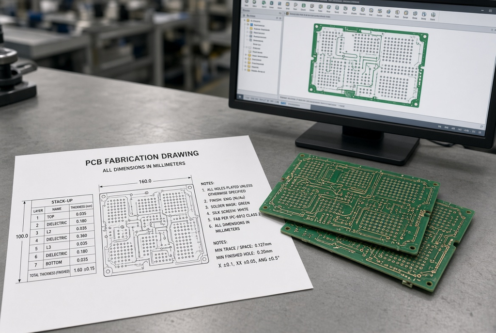
A controlled document that combines Gerbers, drill data, stack-up, and any special requirements, and is the document a fabricator can build from is a PCB fabrication drawing. The geometry of copper, mask and legend. The drawing is not without purpose: revision control, materials, finished thickness, surface finish, via structure, impedance and the notes that don’t fit on a copper layer.
When the Gerber set is complete many teams go ahead without the drawing. That’s how an old revision is released, how “4-layer, 1.6 mm” boards get to lamination with no stack-up, and how expectations go on hold in email. This guide is intended for PCB designers, NPI engineers and sourcing personnel who may need the drawing to be the ultimate source of truth before CAM begars’ questions’.
What a PCB Fabrication Drawing Is (and Is Not)
Note that a fabrication drawing is not an artwork for the file package. When geometry is not sufficient, it is the document that tells how the bare board has to be constructed.
Fabrication drawing vs Gerber and drill files
Gerber files contain image data – copper layers, solder mask, legend and sometimes paste. The hole sizes, slots, plated and non-plated features are defined by drill files. These files are mandatory. They are not adequate.
The fabrication drawing will tie that geometry to the revision, the stack up, the finished-thickness target, the material family, the surface finish, and any special process required. Requirements, when they are only found in a readme or quotation note or in a chat thread, are not controlled. If there is conflict between the two sources, the shop will either guess or stop and ask.
Fabrication drawing vs assembly drawing
A fabrication drawing is a drawing that describes the bare board. An assembly drawing is used to establish the location of components, polarity of parts, keep-out for parts, and mechanical integration after parts are installed.
One mistake that is often made is sending an assembly drawing instead of a fabrication drawing. Assemblers require polarity and reference designators.Assemblers require polarity and reference designators. The fabricator requires copper weight, stackup, outline, finish and via notes. One drawing cannot stand in for the other.
Core Fields Every Fabrication Drawing Should Define
The questions CAM will ask should have been answered in the drawing before it leaves Engineering. The style of drafting is less important that whether the fields below are clear.
Part number, revision, and document control
Indicate board part number, drawing revision, date and which document supersedes if files conflict. An incomplete set includes a complete Gerber with no matching drawing revision.
The typical failure is three PDFs with three dates and no statement of the controlling document. The Gerbers are available in two sets, Rev B and Rev C. The drawing still shows Rev A. The shop constructs the last file received. Include controlling revision on the drawing and do not allow the export to be associated with another release.
Board outline, dimensions, and critical mechanical features
Show a clear board outline, overall size, cutouts, slots, and mounting features. Dimension the interfaces that actually matter: connector edges, press-fit zones, enclosure datums, and keep-outs that affect routing or scoring later.
Tolerances belong where a mechanical interface will fail if they are missed. They should reflect the design and the fabricator’s capability, not a generic title-block default copied from another product.
Layer count, stack-up, and finished thickness
Demonstrate a clear board outline, overall size, cutouts/slots and mounting properties. Measure the interface dimensions that matter such as connector edges, press fit areas, enclosure datums and keep-out areas that will impact routing or scoring later.
Tolerances should be placed where it is likely that a mechanical interface will not work if it is not met. They should mirror the design and show the fabricator’s skill and not be a generic title-block from another product.
Copper weight, material, and thermal requirements
The most frequent source of engineering questions. The drawing should identify layers to be used, thickness to be achieved, and reference to the stack-up table either on the drawing or by name and revision in a separate document.
Without indicating material direction or layer function, it is not a construction “4-layer, 1.6 mm”. It is a hope. You can’t laminate from hope.
Surface finish, solder mask, and legend requirements
Name the surface finish (HASL, ENIG, OSP, or another agreed finish), solder mask color, and legend requirements. If pads must remain free of mask, if legend cannot enter a keep-out, or if a specific finish is required for wire bonding or fine-pitch assembly, write that down.
Choosing finish in email after the job has been planned from an older note is a reliable way to rebuild a traveler. “Finish TBD” is not a fabrication instruction.
Via structure, impedance, and special process notes
Through vias can often be inferred from drill and pad stack. Blind vias, buried vias, via fill, via-in-pad, tenting rules, impedance-controlled layers, and test coupons cannot. Those requirements belong on the drawing or in a referenced document with the same revision.
Special processes follow the same rule: heavy copper, controlled-depth milling, specific electrical test coverage, or a coupon the customer will measure later. If the shop has to assume it, the assumption will be the cheapest interpretation that still looks plausible.
Core fields a PCB fabrication drawing should define
| Field on the drawing | Why it matters |
| Part number, revision, date, and controlling document | Prevents building to the wrong revision or mixed files |
| Board outline, key dimensions, and critical features | Defines mechanical interfaces and tolerances |
| Layer count, stack-up reference, and finished thickness | Locks the construction before lamination |
| Copper weight and material family | Affects lamination, drilling, thermal behavior, and cost |
| Surface finish, solder mask, and legend | Defines solderable surfaces and visual requirements |
| Via structure, impedance, and special notes | Captures advanced requirements that Gerbers alone cannot show |
Stack-Up and Impedance: Where Drawings and Engineering Collide
Stack-up and impedance are where a PCB manufacturing drawing most often stops a job. Geometry can be clean and the construction still undefined.
How to reference stack-up without over-constraining the build
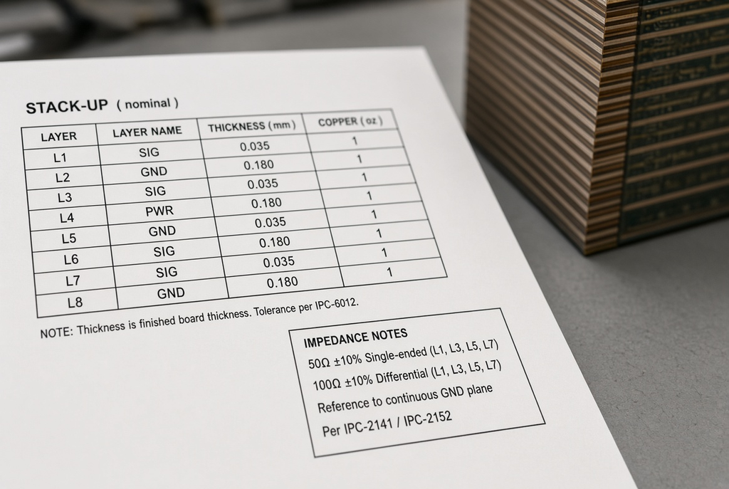
Two approaches work in practice. One is a stack-up table on the drawing: layer name, function (signal, plane, mixed), copper weight, and a thickness target. The other is a separate stack-up document referenced by file name and revision.
Define what the product needs: layer count, which layers carry impedance, dielectric targets that affect impedance or thickness, and the finished-thickness window. Leave internal core and prepreg sequencing to the fabricator unless a qualification or a previous build has locked that sequence.
A stack-up that names layers but not thickness or material direction still generates questions. A stack-up that conflicts with the Gerber layer count generates a stop. Count the copper layers on the drawing against the Gerber set before release.
Impedance notes that fabricators can actually use
An impedance control drawing PCB note is usable when it states the layer, the target impedance, single-ended or differential, the reference plane or planes, and whether a coupon or other verification is required.
“Control impedance” with no layer and no ohm value is not a requirement. It is an invitation to guess. Tolerances should follow the design and the process capability of the shop that will build the board. Publishing a universal tolerance on every drawing does not make the stack-up more manufacturable.
Common Pitfalls in PCB Fabrication Drawings
Most delays on otherwise clean jobs start in the drawing notes, not in the copper.
Missing or conflicting revision information
Symptoms are familiar. CAM imports Gerbers dated Tuesday. The drawing PDF is from last month. The stack-up file has a third date. Nobody wrote which document controls the build.
State the controlling revision in one sentence on the drawing. Export Gerbers, drill, stack-up, and drawing from the same release event. If a file must be updated after release, bump the revision and send the set again as a set.
Vague or generic notes that invite interpretation
“Standard fabrication,” “typical tolerance,” and “impedance as required” look tidy and do no work. The shop will apply its house defaults. Those defaults may not match the enclosure, the connector, or the high-speed pair.
Replace generic notes with a value, a referenced specification, or an attached stack-up. If a requirement is still being decided, do not release the drawing as if it were decided.
Over-constraining construction without need
The opposite error is a drawing that dictates every core and prepreg in the press book when the product only needs a finished thickness and a set of impedance targets. That limits which materials the shop can pull, raises cost, and still does not guarantee better electrical results if the original sequence was copied from another design.
Define performance and the constraints that are truly critical. Leave construction details that do not affect function to the fabricator unless a prior qualification requires the same build.
A Practical Fabrication Drawing Checklist
Treat the drawing as a PCB drawing checklist, not a last-minute PDF export.
Pre-release checks for revision, stack-up, and special requirements
Before the package leaves engineering, confirm:
- Part number and revision match across drawing, Gerbers, drill, and stack-up.
- Layer count on the drawing matches the Gerber copper layers.
- Finished thickness and material family are stated.
- Copper weight is stated for outer and inner layers if they differ.
- Surface finish, mask color, and legend rules are explicit.
- Via type, fill, tenting, or via-in-pad needs are called out.
- Impedance layers, targets, and reference planes are listed if the design is controlled.
- Special test, coupon, or process notes are on the drawing or in a referenced file with the same revision.
That list does not replace a DFM review. It stops the questions that should never have been questions.
Aligning drawing, Gerbers, and drill data
Check the package as one unit. Outline on the drawing should match the mechanical board outline in the Gerbers. Drill hits should land on the pads they belong to. Slots and cutouts should appear in both the mechanical view and the mill or route data. Notes should not forbid a feature that the Gerbers clearly include.
Use one controlled export so Gerber and fabrication drawing files always belong to the same revision. Hand-editing one PDF after the CAM netlist was generated is how mixed packages are born.
Frequently Asked Questions
What is a PCB fabrication drawing and why is it needed?
It is the document that states how the bare board should be built: revision, outline, stack-up, materials, thickness, finish, vias, impedance, and special notes. Gerbers show shapes. The drawing states intent. Without it, the fabricator has to infer construction from geometry and stray emails.
What information should be included in a PCB fabrication drawing?
At minimum: part number and revision, board outline and critical dimensions, layer count, stack-up reference, finished thickness, copper weight, material family, surface finish, mask and legend, via structure, and any impedance or special process notes. If a field affects lamination, drilling, plating, or test, it belongs on the drawing.
Is a fabrication drawing still needed if I have Gerbers and drill files?
Yes. Images and holes are defined by Gerbers and drill files. They don’t consistently deliver finished thickness, material grade, finish option, controlling revision or impedance targets. Those are bare board fabrication requirements and should be put in the drawing.
How should stack-up and impedance be documented?
Draw a stack up table or reference a stack-up table by name and revision on the drawing. Impedance: Indicate layer, target value, pair or single-ended, reference plane and any coupon requirement. Don’t use notes that just read “control impedance”.
What are the most common mistakes in PCB fabrication drawings?
Conflicting revisions, generic notes, no layer count with stack-up, finish as TBD, no layers and no targets called out for impedance. The other common error is specifying the exact press sequence where it is only the electrical performance that is important.
Who should review the fabrication drawing before production release?
PCB designer who owns the stack up, NPI or manufacturing engineer who will be answering CAM questions and the person who releases the purchasing package. If the sourcing is quoting multiple shops from the same files, that reviewer should check to be sure that the drawing and Gerbers are the same revision.