No specific set of PCB panel sizes for all work at all factories. The laminate sheets that are available, the number and thickness of the laminate stack-up, the travel and tooling requirements of imaging, drilling, lamination and test equipment, and the amount of board area that can be used up without touching process margins all determine the layout of a production panel. You should assume that a “standard panel” is a set and fixed paper size and you will have the wrong idea about cost, lead time and what the factory can actually run.
Factories do not come in a standard sheet format. Customer boards are not necessarily boxed into a neat grid, they are placed into larger panels for yield and process control. The important question to ask isn’t, “What is the standard size?” This is the way a fabricator will design their production panel for this material, this outline, and this delivery format.
Customer Panel vs Production Panel: Two Different Things
There’s a lot of confusion that begins with one word: Panel. It is used by designers, buyers, and fabricators; and they may have different objects in mind. If separation of these two objects occurs, there will be a discussion about size, if not, it is talking in circles.
What the customer sees: delivery format and assembly panel
The format boards leave the fabricator in and enter assembly is the customer panel. It can be one board in a bag, a small array specifically designed for a certain SMT line, or a larger delivery panel that will fit with the assembler’s existing depaneling fixture. The drivers are handling, polarity marks, assembler to see fiducials, board separation and lot packing and counting.
This panel is a logistics and assembly decision. They are sized to be easily picked up by the operator or machine, and printed paste on them, placed parts and removed individual circuits without conflict with the outline. It isn’t necessarily the same rectangle that the fabricator used when imaging and drilling the copper.
What the fabricator uses: large production panels for multiple processes
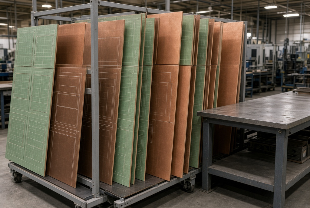
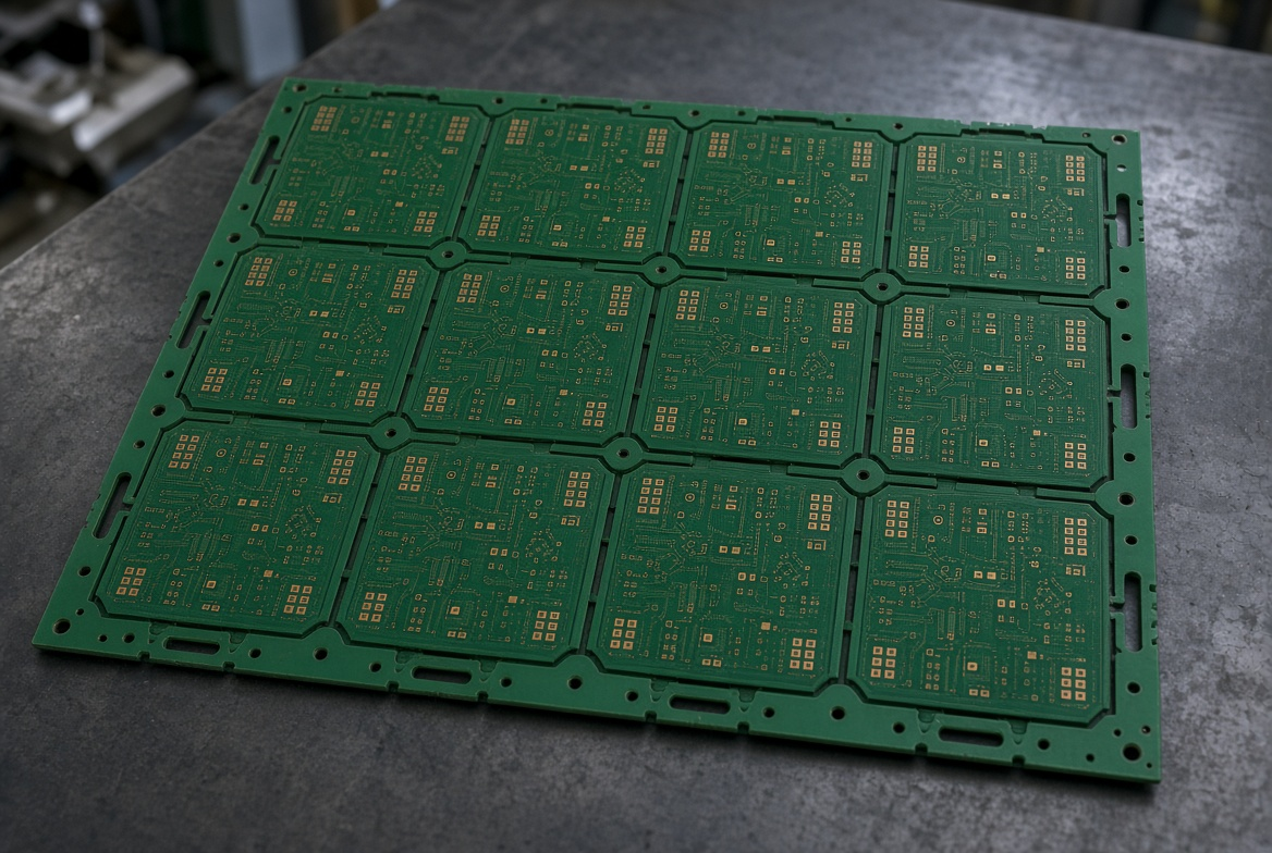
The production panel PCB is a work-piece that is processed in the interior. The larger sheet goes through imaging, etching, drilling, lamination (for multiple layers), plating, solder mask, surface finish and electrical test. Many copies of the same design may be on one production panel. On certain jobs it could be more than one customer’s work, if the material, thickness and process window are compatible.
The shop has designed its plans so that the panel makes it to each station without any damage done to the process margins, tooling holes, coupons, or rails. For most commercial jobs the customer does not need to be very detail on that inside panel. The common first error is to assume that the delivery array is equal in size to the production panel and that is why they are locked in a “panel size” that the factory was never meant to produce.
How Fabricators Plan Production Panels Around Materials and Equipment
The size of the panels is not selected from a catalogue and then imposed on the work. It’s a legacy of machine and material formats. Thus, two quotations for the “same” board may specify two different board strategies.
Laminate sheet sizes and material availability
The sheet is the starting point for planning. Rigid jobs are copper clad laminate that start in the format the mill supplies and the factory has. The number of layers, thickness of cores, prepreg type and copper weight all affect the type and size of sheets that can be employed and their reduction to production panels.
A four-layer board on a common FR-4 core is not going to use material as much as a thicker high-Tg stack or a heavy-copper construction would. If the laminate type is available only in some of these pieces of laminate, or if the sheet on the shelf is already cut to a working size, the production panel must fit within this rectangle. PCB laminate sheet sizes are thus a plan item and not a footnote. If a team assumes that they will always have a dielectric they will find out too late that the shop has to wait for the material or change the nest.
Equipment travel, process margins, and tooling
All stations have a working envelope. Space is required around the circuits for imaging, drilling, presses, routing, and test fixtures: clamping, tooling holes, thieving/border copper as required, and a border to keep the outer traces away from the raw edge. Those increase the size of the area within the production panel, but it is not usable.
The actual travel and the actual width of the border are part of that factory’s equipment and process, and not part of an industry constant. If everyone used one set of numbers, it would be misleading to publish those numbers. The principle that will be transferred between shops is usable area is smaller than the raw panel and a design that does not account for that border will not nest as the drawing implies.
Panel Utilization: Balancing Yield, Cost, and Quality
With the sheet and the envelope of the machine known, the next question is: How many good circuits can be done without making the rest of the process worse? It’s the utilization of the PCB panel, it is a trade, not a score to be maximized at any expense.
What panel utilization means in practice
Utilization is the percentage of the production panel which is converted to shippable board (excluding rail/board, and coupon/board). The more a material is used the lower the process and material cost per circuit. The limit is a physical, not a theoretical one: clearances between outlines, space for break features, panel space for fiducials and tooling, and stiffness to prevent panel from warping and chattering in process.
Efficient nesting viewing on a screen can lead to no safe way to depanel eggs, no test probe and an outer circuit too near the edge of the press or conveyor. A panel that is a good picture in a utilization plot that scrapes edges for routing is not a cheap panel. This is a Quality Problem that is delayed.
When lower utilization is the right choice
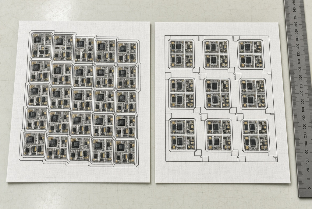
Some buildings are required to return some space. Heavy copper requires a greater amount of process room and thermal mass within the panel. Layered structures with impedance control are frequently required to use coupons and more stable copper balance. A tight nest is easily broken if there are fine features near the board edge, odd outlines or mixed thicknesses. Those are the cases where it’s a better deal to have a simpler circuit plan with wider rails and less circuits per panel, since scrap and rework is more costly than unused rail.
Design Implications for PCB Designers and Buyers
Panel planning is helpful when a drawing or purchase decision is modified prior to the freezing of the Gerbers. That’s the idea behind panel-aware PCB design – make your small outline decisions early, and avoid some big surprise later.
Board size and outline decisions
Add or remove an entire column of boards – a few millimetres in length or width. An outline selected for enclosure convenience may result in a waste of a strip of laminate that could contain another row of enclosure. It’s the same with the reverse: extending a board to utilize the space may push it beyond the machine’s capacity or make a thicker rail which are hurtful to assembly handling.
The problem is, there’s a tendency to attach the outline to the enclosure model and never ask yourself how the rectangle will lay on a sheet. An outline that looks like “the factory is expensive” is often that kind of cost/schedule surprise.
When to let the fabricator own the production panel
For most commercial rigid board products, the customer should specify the single board outline, the delivery format, which assembly requirements the SMT line cannot do without, etc. The fabricator should then have ownership over the circuit production panel, including the number of circuits on the working sheet, where the tooling is kept, and how the nest utilizes the material lot.
The split benefits if the shop is targeting a quantity, a desired ship format (singles or arrays), assembly notes like fixture or handling limits, and notes for special processes like controlled impedance or heavy copper. Then, the factory suggests a panel plan rather than the customer designing it based on one from a search result. The easier the drawing set to review, the easier it is to plan how a fabricator is going to assemble the PCB panels.
Common Pitfalls in Thinking About PCB Panel Sizes
The same three errors are found in RFQs and design reviews. Each is less costly to catch on a call before the stack-up is cut.
Assuming a fixed “industry standard” panel size
One could search for a standard PCB panel size and then draw the product around it, which yields mismatched quotations. Working panels may be cut from a different format of sheet in one shop. A second might retain more border for a press or a test fixture. The difference between customer panel and production panel is eliminated, and there is a debate on a dimension which was not common.
Take into account the size of the panel, it could be job-dependent or factory-dependent. Discuss how this material and this outline will fit into one another. Do not begin at a rectangle that has been published and backwork it.
Optimizing for utilization without considering assembly and test
A filled nest still has a chance to fail at the following building. A printer will bend by the width of the rails. Assembler may not see the fiducials which were suitable for fabrication. Break features that were fine on the fabrication drawing may result in a ragged edge on the final product, which may not pass incoming inspection at the SMT house.
The utilization should be considered along with the delivery format, depaneling method, and test access. If those three are not named, the “efficient” panel is efficient for just one department.
Changing board size late in the project
The current nest can be retired due to a late outline change, or a change in the number of layers that forces a change in the material. Tooling holes move. Coupon placement changes. The sheet format that once worked will no longer produce a meaningful count. This is not a problem of stubbornness on the production line. This is a new panel plan.
Do not increase or decrease the number of layers or board size until the end of the process unless the board function is truly being impacted. The dimensions of the outline should be sent in advance of the shop releasing material if it needs to move.
Pre-Project Checklist for Panel-Aware Design
The majority of the above arguments can be prevented by a short list prior to the fabrication package going out. It doesn’t involve additional forms. It’s the info the individual cutting the sheet truly requires.
Clarify delivery format, quantity, and assembly constraints
Record the desired quantity range, rather than the first prototype purchase. Indicate if singles, a small array of panels or a delivery panel to match an existing fixture is desired. Describe the desired depaneling technique in a non-technical manner; and any handling restrictions that the SMT line currently has: Maximum panel size the printer will accommodate, Keep-out for edge clamps, Polarity markings that are necessary after the panel has been singulated.
These are the special processes also that should be included: impedance coupons, heavy copper, unusual via structures, edge-sensitive components. The notes affect the density of a nest. That’s how they get lost, by not putting them in an email thread instead of in the fabrication notes.
Align cost, lead time, and panel strategy
Check if a row or a column (or both) can be added or deleted to the outline without altering the function. Inquire if the types of materials or thicknesses restrict the types of sheets the shop can cut. Sometimes, if the schedule is short, a simple nest on an easy sheet will come through quicker than a fancy nest on a special cut.
There is a correlation between cost, time and panel strategy. This is not an option, because it does not lead to a lower unit price (based on a fragile nest) nor does it lead to a faster date (based on a material that the mill is not able to provide in this format).
Frequently Asked Questions
Is there a standard PCB panel size used by all fabricators?
Do all fabricators use the same size PCB panel?
The formats, stock, layer numbers and equipment envelopes vary from factory to factory and job to job. A number that was successful in one program is not a standard that must be adhered to in the next shop.
What is the difference between a customer panel and a production panel?
The customer panel is the format for the customer to receive or send to assembly: a single board or an array for handling and depaneling. The production panel is the larger inner panel which the fabricator passes through imaging, drilling, lamination, and test. They can provide each other with a outline. Often, they don’t share a size.
How do fabricators decide how many boards to put in one panel?
They work from the usable area of the working sheet, taking into account process margins, tooling, and fitting as many good circuits as the outline will allow without compromising the assembly, test, or quality. That count can be lower than the mathematical maximum due to material availability and other special processes.
Can small changes in board size really affect cost and lead time?
Yes. If the length or width of the nest is changed slightly, this can either increase or decrease one row or column in the nest, or the panel can be pushed too far over a machine or sheet. This alters the number of times the process cycle is repeated and whether or not the shop can utilize existing material on the floor.
Who should design the production panel: the customer or the fabricator?
For most rigid jobs that are done commercially, the customer should specify the board outline and the delivery format. The production panel needs to be designed by the fabricator. Access to the internal nest by the customer should only be necessary if required by assembly fixtures or contractual panel drawings.
What information should I share with the fabricator about panel and delivery format?
Provide quantity range, preferred ship format, assembly handling limits, intended depaneling method and any special process requiring the use of coupons and additional margin. This is sufficient to allow the shop to suggest a production-panel plan to review rather than making an educated guess as to the size.