The printed circuit board printed with the solder mask is actually a laminated stack of copper, legend, solder mask and dielectric with the plated holes connecting the layers. Traces, pads, vias, planes and the layers on which they reside are the primary components of a circuit board. That’s where the components are placed. Not the board itself.
Not all shapes are traces, not all holes are vias. A plane or a pour of some copper. In some instances holes that are meant to mount, but don’t connect to electricity. When you can identify those features on a real board, and on a fabrication drawing, you can determine if the files represent a buildable stack Teams that need that stack produced from Gerber data and a drawing work through PCB fabrication.
Traces: The Routed Conductors
A trace is the copper trace used to convey a signal or a power current from one point to another. It will appear as a thin line under the solder mask on a completed board. On a Gerber layer it is the routed copper that is not a pad, a via pad, or a plane.
Width and spacing are not drawing decoration. The current, voltage drop, and in the case of high-speed nets the impedance the stack-up is intended to comply with determine the width. The space between is determined by the voltage, etching ability, and allowed spacing between the next feature. Those geometries are etched from copper foil by a fabricator. Normally, if the artwork requires a line the process cannot hold, the board will return to the boardroom “green and complete” with opens, near-opens or impedance that is not on record on the drawing.
The examples on the shop floor are uninteresting. A 12 V rail with a smaller width of trace will cause heat to accumulate in the copper and the laminate surrounding it, if it is driving a motor driver with a current rating higher than the current flowing through it. If the differential pair is routed with a varying separation or if the reference plane is lost down the center of the pair, it will not perform as the layout tool indicates it would. Both problems have no mystery after assembly. In both the copper layer and the stack-up, these were clearly present in the existing structure.
What a fabricator must see on the drawing
The drawing and fabrication notes need to contain answers to three questions before the board is made:Before the board is made, the drawing and fabrication notes must have answers to three questions for each copper layer that has routed conductors:
What is the least trace and space that layer can have? The note and the art work have to match. One of the most frequent mistakes is to get the outer line and space at 3 mil and then talk about “making it work” when in fact, it doesn’t work. What the process window allows is what can be held by a fabricator. Hope is not the correct response if the files and process do not match, it’s a design change or a process discussion.
Second, do any of the nets include controlled-impedance pairs or controlled-impedance singles? Those traces require a reference plane, a defined dielectric and target impedance. The pair geometry should be included in the artwork. The intent of the target and its layer assignment should be in the stack-up note.
Third, what is the clearance between the edges of the copper? The traces that run to the board outline or that fall within the routing tab keep-out are damaged during scoring or routing. This is a drawing problem, not a handling problem afterwards.
Use the same hand to read the trace layer with the stack-up. A thin high-speed pair on an inner layer without a continuous reference is not a ‘flourish’ for routing. It is a partial interconnect.
Pads: Where Parts and Contacts Land
A pad is the exposed copper surface to which a part lead, solder ball, connector pin or test probe contacts. It’s the only copper that most people can solder. All other parts of the mask are covered by the mask unless the designer had opened it on purpose.
Through-hole pads are copper around a drilled hole that is annular in shape. The lead passes through the hole and the solder fills the barrel and wets the pad on one or both sides. SMT pads are copper lands that are located on top surface. Part is placed on paste, and the termination is reflowed wet with the paste. Solder mask opening is typically smaller than copper pad. That overlap is the edge that is defined by the mask or by the copper; the edge you see on a completed board.
Just viewing the layout canvas, a pad may appear to be completed while the mask layer is still present. Both the copper Gerber and the mask Gerber need to be read in conjunction. If there is no opening in a thermal pad under a QFN, it is not a soldering surface. It is copper that is contained within the polymer.
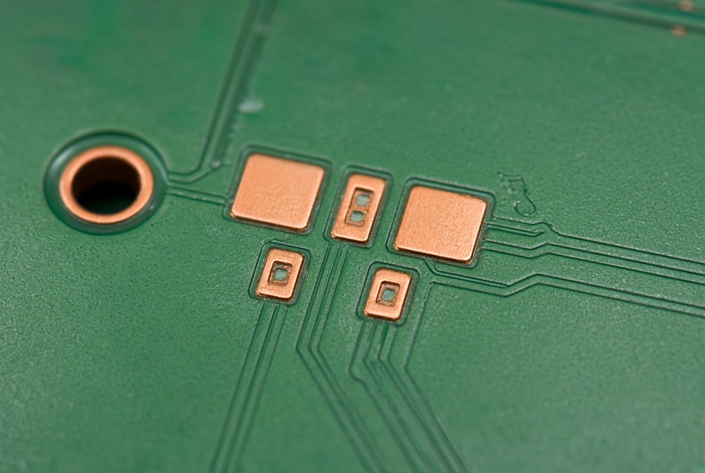
Pad shapes and assembly constraints
Rounded, rectangular, oblong, and thermal-relief are the typical shapes of common pads. Through-hole leads and some connectors have round and oblong shaped pads. Chip components and many IC leads are rectangular pads. Thermal-relief pads are small islands of copper that are glued onto a plane with a short piece of copper with the joint to be heated by the iron or reflow oven, but not absorbing all of the heat.
Shape is a constraint, it is not a choice for the aesthetic. The volumes on a small rectangular pad must be pasted to match the termination. A pad that is too big allows the part to float. A pad that is too small will deprive the joint of nutrition. A thermal pad without relief in a power package, or having vias that pull solder into the barrel, will be difficult to wet during reflow and even more difficult with a hand iron. The BGA and QFN rules are the same: leave a circle of copper and mask opening for the ball or the center pad to land on.
PCB pad design for assembly is decided on the bare board. The assembler can only work with the openings and the copper you released. When the question shifts from “does this land look right in CAD” to “can this land take solder,” the next conversation is PCB assembly for SMT or through-hole mounting on those pads.
Vias: Plated Connections Between Layers
A via is a hole that is formed between two copper layers. The drill is a cutting tool that removes material. Plating grows copper on the barrel. Each connected layer is provided with annular rings, which provide something to tie into the barrel. This is an electrical connection between layers.
There is a through via from the top of the stack to the bottom. Inside materials can only be allowed to be blind and buried vias. Microvias are small laser-drilled holes in sequential build up. Those structures involve different drill strategies, plating sequence and cost. They don’t require an entire lecture to be properly named. The use of the term “microvia” for a 0.2 mm through hole is incorrect even though it is a small hole.
Fabrication method of PCB involves using via types, which is a construction choice. One through via on a typical multilayer press is one drill and one plating operation. Sequential lamination, or controlled-depth drilling is added to make blind and buried vias. That’s why a via is never “just a hole” on the quote.
When a via is not just a hole
It can be finished open, tented or plugged. In an open via, there is a mask opening over the hole. The barrel is susceptible of flux and solder entering it. Solder mask is used over a tented via. Plugged or filled via is a barrel filled with resin or conductive filling material sometimes plated on top for a pad.
The selection is made based on assembly and impedance. Vias that do not close in a pad field will be a source of solder theft. If the vias remain open under a high-speed pad they can form a stub or void in the solder joint. The via is often used for tenting when the via does not need to be soldered and is only used to connect layers. Plugging is used in both of the following cases: A via located in a pad or When the barrel will not contain chemistry or air.
Two assumptions cause most drawing fights. The first is that every via is open on both sides because that is how the 3D view rendered. The second is that any small via is a microvia. A small mechanically drilled through hole is still a through via. Call the structure by how it is built, then put the drill size, the spanning layers, the annular ring, and the tenting or plugging note on the fabrication drawing. Readers who are writing those notes can use the PCB design guidelines for via structure, annular ring, and drill callouts a fabricator can actually build.
Planes and Copper Pours
Not every copper is fed into thin traces.Not every copper goes into a thin trace. A flat piece of copper for power or ground. Unused space on a signal layer is filled with a copper pour which is generally connected to a net, typically ground. Planes and pours establish return paths, manage impedances and distribute heat. They also affect the way the board etches and how the stack laminates.
A plane is the large copper which can be seen on a finished board when holding the board to the light on an inner-layer coupon or the solid pour underneath the mask on an outer layer. On the Gerber it’s a flood, not a snake of routes. A via or a through-hole pad meeting a plane can be a part of that flood. Otherwise, the pad is difficult to solder. If they’re too fast, there’s a low bond between the plane/human.
What can go wrong with pours and planes
The first problem is isolated copper slivers. A wave that passes between traces may result in an unnetted thin peninsula. That is a thin section which may be uneven and can pull up. Acid traps are sharp inside corners which acid will be stored. Lamination and etching is more difficult to control due to uneven copper (wide pours on one side, low traces on the other). The press has different resin flow. The etcher is subjected to other loading.
Most of those defects are due to two drawing habits. For a layout that has a large un-used copper, it is neat and will be a loose conductor after etch. If the routing path is not separated from the edge of the board by a copper keep-out, the foil will be routed into it. Set the net, pour clearance to traces and to outline, and Thermal Relief style. Now view the poured layer as a copper balance problem, not just as a ground symbol, like a CAM operator would.
Layers and Stack-Up
One copper plane in the stack is a layer. In reality, what is a PCB layer? A 2-layer board is a laminate made of a single dielectric core with copper on both sides. A multilayer board includes one or more internal prepreg layers between signal, power and ground layers. The printed circuit board stack-up is a sequence of the different copper layers and their respective layers of dielectric (material, thickness, and copper weight).
It is not possible to count layers when the photograph is of a green board. The stack is masked with color. Edge plating and a routed edge may indicate a layer count, but the drawing will indicate the layer count. The 4-layer board and 8-layer board can be the same on a desk.
A design moves from two copper layers to a laminated multilayer stack when the interconnect density, the need for a continuous reference plane, or the mix of power and signal can no longer live on top and bottom alone. That construction is multilayer PCB manufacturing, not a thicker piece of the same two-layer process.
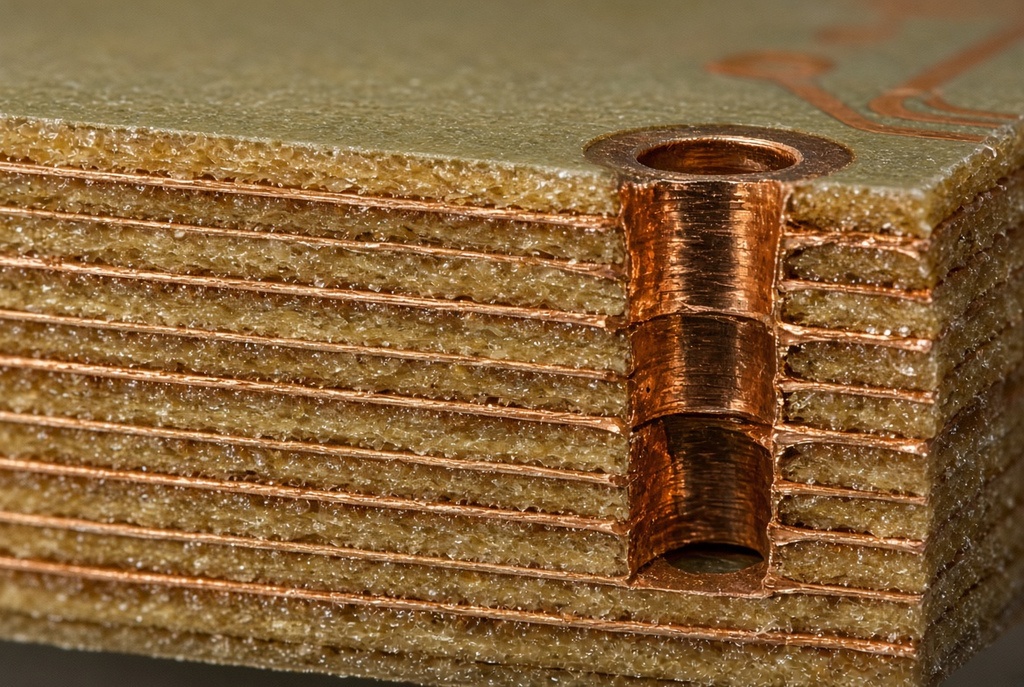
What the stack-up must say
Short and Complete – a usable stack-up note. It includes number of layers, order of the copper layers, the type and thickness of the dielectric between layers, the weight of the copper in each layer, and any impedance targets and the layers they have been used in. If the board uses mixed dielectrics, the board names them. The note indicates if an inner layer is a plane.
That note is a weak FR-4 note. This does not provide thickness, copper weight or target impedance. If the design has controlled-impedance pairs, the omission means either the fabricator has to create a stack or the job must be aborted. Write the stack you want to purchase. Next look to see that the Gerber layer names are consistent with the stack-up names. Inner layers lose their reference when there is no match between the impedance setting in the table and the GND setting in the file set.
Solder Mask, Legend, and Surface Finish
Solder mask, legend, and surface finish are part of the finished bare board. They’re not the electrical stack and they determine what can be soldered and what can be read by the assembler.
The polymer coating that protects copper and exposes openings for soldering or similar is called solder mask. Any assembly notes on the mask or reference designators, polarity marks are printed on legend, or silkscreen. Surface finish is a process applied to the surface of exposed copper that is exposed, and which determines the wetting properties of solder.
The solder mask and surface finish should be included in the fabrication notes along with the copper and the stack-up. Mask colour & mask finish name (no openings) is incomplete, no process matching assembly.
Color, markings, and finish are not the board
Mask color, logo, and a finish marketing name are things that can easily be argued about and are easy to over-specify. Electrical behavior resides in the copper, the dielectric and the stack-up. Two boards (one green, one black) of identical stack and copper content are the same circuit.
Select the end result of an assembly and the shelf life desired, rather than aesthetics in a photograph. If it is a procurement mistake and will oxidize after the SMT run, it will not look good in a photo. Any drawing error is a Legend that is too fine to print or is placed on a pad. Don’t put logos or decorative marks on copper features or in mask openings. After the artwork appears complete, the board must be etched, plated and soldered.
Components: On the Board, But Not the Board
The board has resistors, capacitors, ICs and connectors attached to it. They leave their footprints in the form of pads, keep-outs and occasionally via placement. Parts are supply-chain and assembly decisions. They are not just plain board features.
For that reason this article will not turn into an article that tells you what components are best for each application or model. For physical board readers, the part specifies which pad field to check. When reading a fabrication drawing, the part is only shown as a land pattern and a hole schedule. The BOM and the centroid file are attached to the assembly.The BOM and the centroid file are associated with the assembly. Fabrication includes the copper, drill, mask and stack-up.
When component choice changes the board
To ensure the most competitive bid for the part, some packages will alter the board prior to the ordering of the part. Because of the fine pitch, via-in-pad policy and sometimes due to an additional layer or tighter stack, escape routing leaves the array through a fine pitch BGA. A large connector requires mechanical keep-out, thicker copper (or additional pads in the case of current) and in some cases a support hole that is not a via. If the transformer is heavy or the electrolytic is tall, the through-hole pad must be capable of supporting wave or selective solder and the thickness of the board will not allow it to flex under the weight of the transformer/electrolytic.
The catch is to choose the package first and then order the fabricator to go around it without stack-up. The selection of packages, pad design, via structure and the number of layers must be determined together as one construction. Otherwise, the assembly drawing and the fabrication drawing represent two different products.
A Quick Reading Checklist for a Real Board
Walk the circuit board next to the fabrication drawing, using this list. The art of reading a PCB without taking the photo for the specification.
- Traces: measure width and spacing on each layer and compare to the note. Search for necks, copper-to-edge violations and reference loss of impedance pairs.
- Pads: find the land and the mask opening. Check through-hole vs SMT, and ensure that thermal pads are indeed open.
- Identify Vias first and then write them. Record whether they are opened, tented or stuffed. A small through hole should not be called a microvia unless it is a laser via on a sequential stack.
- Name the net which is made up of planes and pours. Search for slivers on the surface of the board, or missing thermal relief, and for copper that extends to the outline.
- Layers: Number them from the top of the stack, not the photo. Verify the thickness of the dielectrics and weight of copper.
- Mask, legend and finish: check openings, readable markings which do not come in contact with pads and a finish, which is consistent with the desired soldering procedure.
Take that checklist to the fabrication review. As long as the copper, the holes, the mask, and the stack-up on the drawing describe the same thing (object), the board in your hand is correct.